KENBAK-1 · Volume 15
KENBAK-1 — Volume 15 — Building a KENBAK-uino
Mark Wilson's 2011 original, the grey box that every KENBAK emulator kit descends from: how it was built, whether it runs the same code as the nanoKENBAK-1, its schematic, a parts list with today's substitutes, the faceplate and drilling guide, loading the firmware, and programming it
15.1 About This Volume
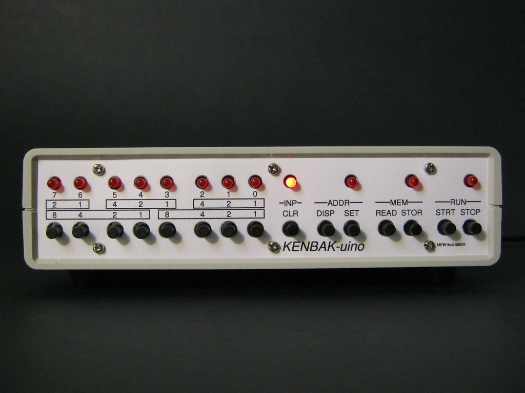
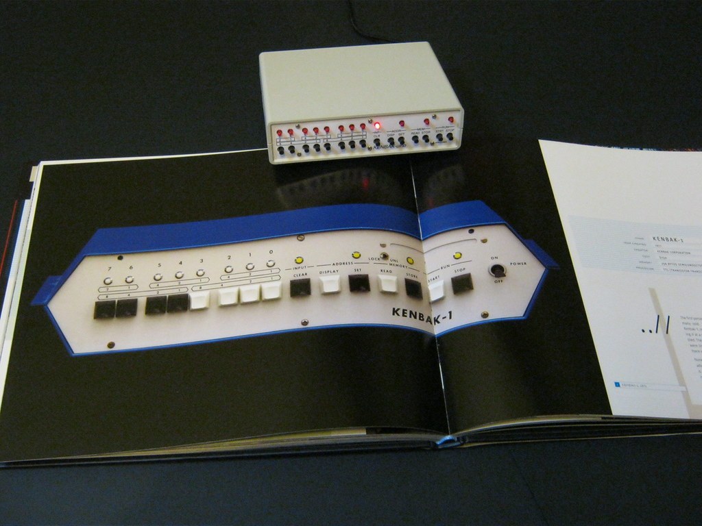
Volume 8 introduced the KENBAK-uino in a paragraph: an Arduino-compatible ATmega328 running Mark Wilson’s emulation of the KENBAK-1, in a small grey box with a front panel laid out like the original. Every emulation kit since, the µKENBAK-1 of Volumes 9 and 13 and the nanoKENBAK-1 of Volume 14 among them, runs a version of the program Wilson wrote for it. This volume goes back to the machine itself and treats it as something to build. I may build one like this as well.
Wilson photographed his build stage by stage in September 2011 and posted the set on Flickr with a short note under each picture (album “KENBAK-uino”). Those photographs, his source code on GitHub (funnypolynomial/Kenbakuino), its ASCII schematic and his PostScript file for the faceplate are together enough to build a close copy, and they are the sources for everything below. The volume answers one question first, whether the KENBAK-uino runs the same code as the nanoKENBAK-1. It then draws the circuit, lists the parts with current replacements, follows Wilson’s construction, and ends with loading the firmware, testing, and keying the program from his video.
15.2 Wilson’s Machine
Mark Wilson, of Christchurch, New Zealand, came to the KENBAK-1 looking for an early computer to re-create with an Arduino. In the notes that come with his code he explains the choice: the Altair 8800 had “30+ LEDs and 20+ switches and seemed like too much work”, while the KENBAK-1 had “only a dozen LEDs and 17 switches. Perfect!” (kenbakuino.txt). The year was 2011, forty years after the KENBAK-1 was first advertised.
He began with the software. The first task, his caption to the design photograph says, was “a C++ class which emulated the Kenbak’s ‘CPU’ and instruction set”, written from scans of the original typewritten manuals. With that working he “moved onto the tricky part: the hardware” (Flickr, “Design & Prototype”).
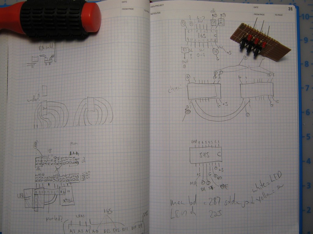
Two decisions shaped the machine. The first was scale: “the sizes of the LEDs and pushbuttons I intended to use … determined the over-all scale of the project and its proportions”, and he found a project box to suit. The second was what to leave out: “I decided almost immediately to discard the Kenbak’s Power and Lock switches”. The KENBAK-uino is powered from its USB cable and has no memory lock.
He prototyped the switch and lamp circuits on a solderless breadboard first. The hardware, his caption says, “is not particularly complicated”: the Arduino reads the buttons through two daisy-chained 74HC165 shift registers, drives the eight data lamps through one 74HC595, and drives the four control lamps directly from its own pins; a real-time-clock module was added so that the machine could also be a clock (Flickr, “Prototyping the Switch Controllers”).
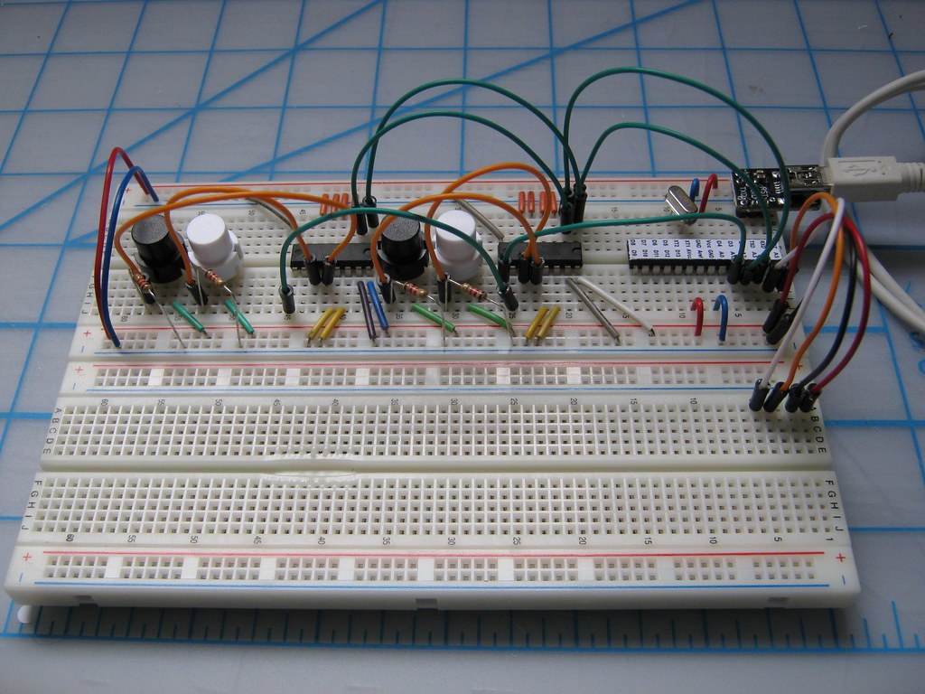
Then he built it for real on perfboard, three small boards and “a lot of work, 500+ solder joints”, squeezed them into the case, “and tested all the buttons and LEDs, amazingly, everything worked first time” (kenbakuino.txt). Most of his time after that went into the software around the emulator, which he calls the MCP (master control program): the built-in programs, the extensions, the clocks. The faceplate is signed “MEW fecit MMXI”: MEW made this, 2011, MEW being Wilson’s initials.
15.3 Is It the Same Code as the nanoKENBAK-1?
Yes, with one setting changed. The answer comes from three sources: Wilson’s repository, Adwater & Stir’s own pages, and the code itself.
- Adwater & Stir say so. The nanoKENBAK-1 page states that it “has the same ATMEGA328p programming from Mark Wilson as the µKenbak-1 (and the full-size version)” (nanoKENBAK-1), and the maker’s software page points to Wilson’s GitHub repository as “the source code for the µKenbak-1” (Kenbak Software Install).
- Wilson says so. His README notes that “you can now buy a kit which uses the sketch”, linking Adwater & Stir.
- The one hardware difference is a setting in the code, not a different program. Wilson’s KENBAK-uino uses a DS1307 clock chip (Library copy); the µKENBAK-1 and nanoKENBAK-1 use a DS3231. The firmware handles both:
Clock.hhas a small table of three constants,RTC_I2C_ADDR,RTC_CONTROL_OFFSETandRTC_USER_SRAM_OFFSET, with rows for no clock at all, the DS1307, the DS3231 and the DS3232. The repository ships set for the DS1307 (0x68, 0x07, 0x08); Adwater & Stir’s install page gives the DS3231 values (0x68, 0x0E, 0x00) to build it for their kits.
What changes with that setting is where the firmware keeps its eight bytes of settings (the auto-run choice, the key-toggle flag and five user bytes). The DS1307 has 56 bytes of battery-backed RAM, and the firmware puts them there. The DS3231 has none, so with RTC_USER_SRAM_OFFSET at 0 the firmware reserves the top eight bytes of the ATmega’s EEPROM instead (Memory::GetEEPROMTopIdx() in Memory.cpp). Everything else is the same: the emulated processor (CPU.cpp), the front-panel logic and extensions (MCP.cpp), the eight built-in programs, the serial loader and the pin assignments.
Table 1 — Is It the Same Code as the nanoKENBAK-1?
| KENBAK-uino (Wilson, 2011) | nanoKENBAK-1 / µKENBAK-1 (Adwater & Stir) | |
|---|---|---|
| Program | Wilson’s Kenbakuino sketch | The same sketch, built by the maker |
| Processor | ATmega328P, 16 MHz, Arduino Uno bootloader | ATmega328P |
| Clock chip | DS1307 module (SparkFun) | DS3231 |
Clock.h | as published: 0x68 / 0x07 / 0x08 | 0x68 / 0x0E / 0x00 |
| Settings stored in | the DS1307’s RAM | top 8 bytes of the ATmega’s EEPROM |
| Buttons and lamps | 2 × 74HC165, 1 × 74HC595, 4 direct | the same arrangement (Volume 13) |
| Power and lock toggles | none | µKENBAK-1: power toggle; no lock |
Two cautions keep this from being a perfect identity. First, the maker has never published his kit builds as a separate source or version, so the exact build in a given nanoKENBAK-1 is not known: Volume 13 records that early µKENBAK-1 firmware read a memory-lock input on D7 that Wilson’s code does not have, and the maker’s booklet gives a different power-on speed from Wilson’s notes. Second, Wilson has kept fixing the emulator: the May 2021 change made right shifts keep the sign bit, as the original does, and the September 2022 change advanced the program counter after each instruction instead of before. A kit flashed before those dates behaves slightly differently from a KENBAK-uino built today from the current source. Volume 9’s acceptance program tests both in under a second on any of them.
So a program written for one runs on the others, the built-in programs are the same on all of them, and a KENBAK-uino built with a DS3231 instead of a DS1307 is, in software, a nanoKENBAK-1 in a different box.
15.4 The Circuit
Wilson’s schematic is an ASCII drawing in the comments of PINS.h, corrected in May 2025 to show the data-lamp order as actually wired. The drawing below redraws it with the real pin numbers of the three chip types, and adds in dashed orange the handful of parts that his parts list leaves out because any working ATmega328 circuit has them.

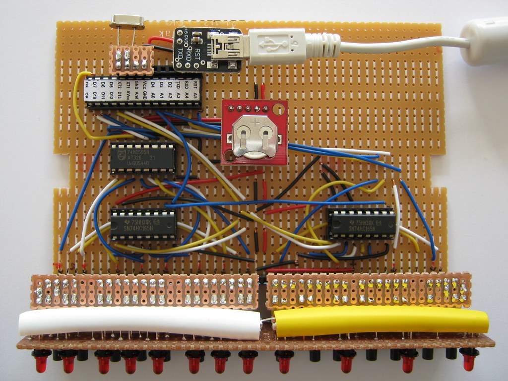
The processor. An ATmega328P, the chip of the Arduino Uno, with a 16 MHz crystal and the Uno’s bootloader, so that new firmware arrives over the serial port. Wilson socketed even the crystal: “So modular even the XTAL is socketed. I kinda hate to commit something non-trivial to a permanent solder joint unless I have to” (Flickr, “Populated”).
Power and USB. A small USB-to-serial adapter board, with pins labelled +5, GND, RXD, TXD and RST, gives “USB for power and sketch updates” (same caption). The whole machine runs from the computer’s or a charger’s 5 V. There is no regulator, no power switch and no fuse.
The data lamps. The 74HC595 is a serial-in, parallel-out register: the processor clocks eight bits into it and latches them onto its outputs, each of which lights one lamp through a 220 Ω resistor. Wilson wired output Q0 to the leftmost lamp, bit 7, so the firmware shifts the byte out least-significant bit first. The PINS.h note says either order is fine as long as the code matches: wire Q0 to bit 0 instead and change LSBFIRST to MSBFIRST in LEDs::ShiftOut().
The control lamps. INP, ADDR and MEM come straight from pins A1, A2 and A3. RUN is on D11, a PWM pin, so that a program can dim it: the firmware’s control-lamp system call uses four bits for the RUN lamp’s brightness.
The buttons. Each button connects its 74HC165 input to +5 V when pressed; a 10 kΩ resistor holds the input low otherwise. The processor pulses the load line (PL) to capture all sixteen inputs at once, then clocks them out of the chain into A0, sixteen bits in two bytes. Fifteen inputs are buttons and the sixteenth is tied to ground.
Wilson wired the buttons to whichever ‘165 input was convenient on his board, and the firmware puts them back in order through a sixteen-entry table, m_pMap[] in Buttons.cpp. To copy his board exactly, wire them as he did:
Table 2 — Wilson wired the buttons to whichever '165 input was convenient on his board, and the firmware puts them back in order through a sixteen-entry table, mpMap[] in Buttons.cpp. To copy his board exactly, wire them as he did
| 74HC165 | D0 (pin 11) | D1 (12) | D2 (13) | D3 (14) | D4 (3) | D5 (4) | D6 (5) | D7 (6) |
|---|---|---|---|---|---|---|---|---|
| #1 (Q7 → A0) | Bit 0 | Bit 1 | Bit 6 | Bit 7 | Bit 4 | Bit 5 | Bit 2 | Bit 3 |
| #2 (Q7 → #1 DS) | STOP | STRT | unused, to GND | CLR | DISP | SET | READ | STOR |
A new layout can wire them in any order that suits the board, and then the table must be edited to match: entry n of m_pMap[] is the bit position (0–15, chip #1 = 0–7) at which button n appears, the buttons being numbered Bit 0 to Bit 7, then Clear, Display, Set, Read, Store, Start, Stop and the unused input.
The clock. A breakout board carrying the DS1307 clock chip, its 32.768 kHz crystal and a backup coin cell, on the I²C pins A4 and A5. “The little red board is the RTC is from SparkFun” (Flickr, “Populated”). The I²C pull-up resistors are on the module.
What the parts list leaves out. Wilson’s component list in PINS.h is the parts that make it a KENBAK: the chips, the clock module, 12 LEDs, 15 buttons, 12 × 220 Ω, 15 × 10 kΩ and the crystal. A bare ATmega328P also needs two load capacitors on its crystal (22 pF each is the Arduino value), a pull-up on its reset pin, a capacitor from the adapter’s reset line so that uploads can restart it, and a 100 nF decoupling capacitor at each chip’s supply. These are drawn dashed. None of them shows clearly in Wilson’s photographs, and none is needed if an Arduino Nano is used in place of the bare chip (next section).
15.5 Bill of Materials
The list follows the circuit as Wilson built it, then gives for each line the part to buy in November 2026 and why it differs, in the format of the series’ other parts lists. Tags: Same, the original part is still a catalogue item; EOL, it is discontinued; Spec, the original line is incomplete or out of a data-sheet limit; Choice, a change chosen for a copy. Stock and prices were read on 2 November 2026 and change daily. A printable version with tick boxes is at the end of this volume (Printable Bill of Materials).
15.5.1 Semiconductors and modules
Table 3 — Semiconductors and modules
| Qty | Where | Original | Buy now | Tag | Why |
|---|---|---|---|---|---|
| 1 | Processor | ATmega328 (DIP-28), Uno bootloader | ATmega328P-PU (Microchip, DIP-28) with the Arduino Uno (Optiboot) bootloader, or an Arduino Nano (below) | Same | Still made in DIP. Buy it with the bootloader already burned, or burn it with an Uno running “Arduino as ISP” (Volume 13, “Rebuilding the Firmware”). A blank chip from a distributor has no bootloader and cannot be loaded over serial |
| 1 | Processor alternative | — | Arduino Nano (ATmega328P, 16 MHz, USB on board) | Choice | Replaces the bare chip, crystal, load capacitors, reset parts and the USB adapter in one board. Its pins D8–D13 and A0–A5 are the same Arduino pins the firmware uses, so PINS.h needs no change. Many clones need the board setting “ATmega328P (Old Bootloader)” to upload |
| 1 | Clock oscillator | 16 MHz crystal (socketed) | 16 MHz HC-49 crystal | Spec | Wilson lists the crystal only; the ATmega also needs two load capacitors, the “Crystal load” line below (neither is needed with a Nano) |
| 1 | Data-lamp driver | 74HC595 | 74HC595 (TI SN74HC595N, DIP-16) | Same | Active. See the LED-resistor line below for its current limit |
| 2 | Button readers | 74HC165 | 74HC165 (TI SN74HC165N, DIP-16) | Same | Active |
| 1 | Clock | SparkFun “Real Time Clock Module” (DS1307, product 99) | SparkFun BOB-12708 (DS1307, CR1225 cell), or a DS3231 module with Clock.h changed | EOL | Product 99 is retired; its successor BOB-12708 is the same DS1307 board, in stock at SparkFun (BOB-12708). It runs Wilson’s code unchanged. A DS3231 keeps far better time (it has a temperature-compensated crystal inside the chip) but needs the three DS3231 constants in Clock.h, as the commercial kits use. Adafruit’s DS3231 breakout (product 3013, CR1220 cell) was out of stock on 2 November; the cheap blue “ZS-042” DS3231 modules work, with one caution in the next line |
| (1) | Clock alternative | — | ZS-042 DS3231 module with a CR2032 | Spec | These modules carry a diode and resistor that trickle-charge the coin cell, meant for a rechargeable LIR2032. At 5 V with an ordinary CR2032 the usual advice is to remove the resistor (or the diode) so that the primary cell is not charged (Arduino forum thread). The advice comes from builders, not the module’s maker; the DS3231 data sheet (Library copy) makes no provision for charging a primary cell |
| 1 | USB power and serial | Small mini-USB serial adapter, pins +5 / GND / RXD / TXD / RST (make not identified) | Adafruit FTDI Friend (FT232RL, product 284, in stock) or any 5 V FTDI- or CH340-type adapter with a DTR or RTS reset pin | Spec | Wilson’s board is not named in his notes. Whatever is used must supply 5 V and bring out a reset signal (DTR or RTS) for automatic uploads. Not needed with a Nano |
| 12 | Lamps | LED, red (3 mm, from the photographs) | 3 mm red LED, diffused, high-efficiency | Same | Wilson’s faceplate holes are 5/32 in (4.0 mm), sized for 3 mm LEDs |
15.5.2 Passive parts
Table 4 — Passive parts
| Qty | Where | Original | Buy now | Tag | Why |
|---|---|---|---|---|---|
| 12 | Lamp resistors | 220 Ω | 680 Ω–1 kΩ for the 8 data lamps; 220–470 Ω for the 4 control lamps | Spec | With red LEDs (about 2 V) on 5 V, 220 Ω asks about 13 mA per lamp. Eight data lamps lit at once (the value 377) then ask about 100 mA of one 74HC595, whose absolute maximum through its VCC or GND pin is 70 mA and whose outputs are specified at 6 mA (Library copy; TI SN74HC595 data sheet, §6.1 and §6.5). The chip’s output resistance limits the current somewhat, which is why Wilson’s machine works, but it runs outside the data sheet. With high-efficiency LEDs, 1 kΩ (about 3 mA each, 24 mA for all eight) is still bright indoors. The control lamps come from ATmega pins rated for 20 mA, so 220 Ω is acceptable there; match brightness by eye |
| 15 | Button pull-downs | 10 kΩ | 10 kΩ, ¼ W | Same | |
| 2 | Crystal load | (not listed) | 22 pF C0G | Spec | Bare-chip build only |
| 1 | Reset pull-up | (not listed) | 10 kΩ | Spec | Bare-chip build only |
| 1 | Auto-reset | (not listed) | 100 nF ceramic, adapter DTR/RST to ATmega pin 1 | Spec | Lets the Arduino software restart the chip for an upload. Bare-chip build only |
| 4 | Decoupling | (not listed) | 100 nF X7R, one at each chip | Spec | Standard practice for every logic chip |
| 1 | Supply reservoir | (not listed) | 10–47 µF, 10 V or more, across the 5 V input | Choice | Steadies the supply at the end of a long USB cable |
15.5.3 Front panel and switches
Table 5 — Front panel and switches
| Qty | Where | Original | Buy now | Tag | Why |
|---|---|---|---|---|---|
| 15 | Keys | Push-button, normally open: black, tall, square body, round plunger (from the photographs) | 6 × 6 mm through-hole tactile switch with a long round plunger, about 13 mm overall | Same | The plunger must pass a 3/16 in (4.8 mm) hole in the faceplate and stand proud of it. Tayda and most suppliers list these by overall height; check the plunger diameter against the hole |
| 0 | Power and lock toggles | — (omitted by Wilson) | Optional: a power toggle in the USB 5 V line | Choice | The original’s lock key protected memory; Wilson’s firmware has no lock input. A power switch is a simple addition |
| 1 set | Faceplate | Wilson’s PostScript artwork printed on heavy paper, holes punched | Print kenbak.ps at 100 % on card or adhesive vinyl; or have it engraved | Same | Section “The faceplate” below |
| 1 | Backing plate | Drilled plastic, behind the card | 1.5–2 mm acrylic or ABS, drilled from the drilling guide | Same | Wilson tried a laser-printed transparency for the labels “but it kept smudging” |
15.5.4 Boards, case and hardware
Table 6 — Boards, case and hardware
| Qty | Where | Original | Buy now | Tag | Why |
|---|---|---|---|---|---|
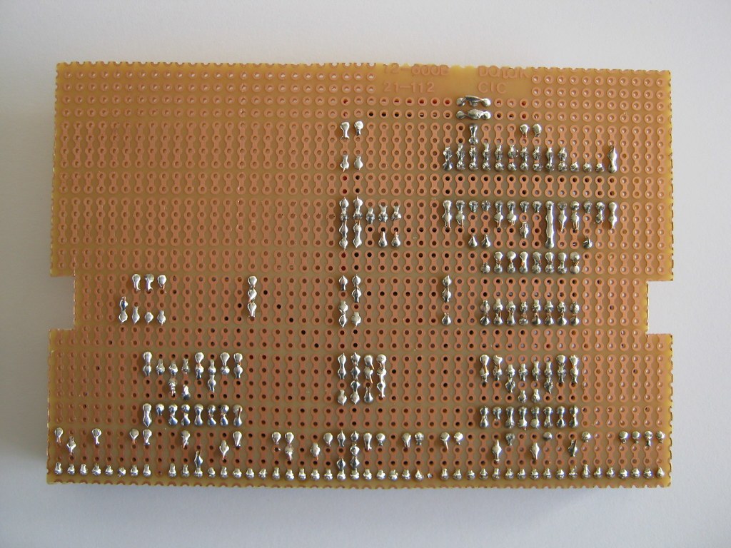
| 3 | Boards | Perfboard, pad per hole; the main board is marked “12-600B Datak” | Pad-per-hole perfboard, 0.1 in pitch, or a small PCB | Same | Wilson: “All the circuits were made with perfboard, the holes provided a convenient grid to help keep everything aligned” |
| 4 | Chip sockets | DIP-28 × 1, DIP-16 × 3 | DIP-28 (0.3 in) × 1, DIP-16 × 3, machined (turned-pin) | Same | Every chip in Wilson’s build is socketed |
| 1 lot | Board-to-board | Header pins and socket strip; long resistor legs | 0.1 in male headers (straight and right-angle) and female socket strip | Same | |
| 1 | Case | Grey ABS instrument case with slide-in front and rear panels and card guides, not named by Wilson | An ABS instrument case about 140 × 110 × 35 mm, e.g. Jaycar HB5970 or Altronics H0472 | Choice | Wilson’s faceplate frame is 135 × 31 mm, which fits the front opening of this common size; Australian and New Zealand retailers stock it. Wilson never names his box, so this is a match by size, not an identification. Check the panel opening of any case against the 135 × 31 mm faceplate before buying |
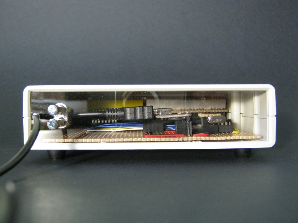
| 1 | Rear panel | Clear plastic (replacing the case’s opaque panel) | Clear acrylic, cut to the case’s rear-panel size | Choice | ”I knew friends and co-workers would want to see the inside, so I switched to clear” (Flickr, “Assembled — Back”) |
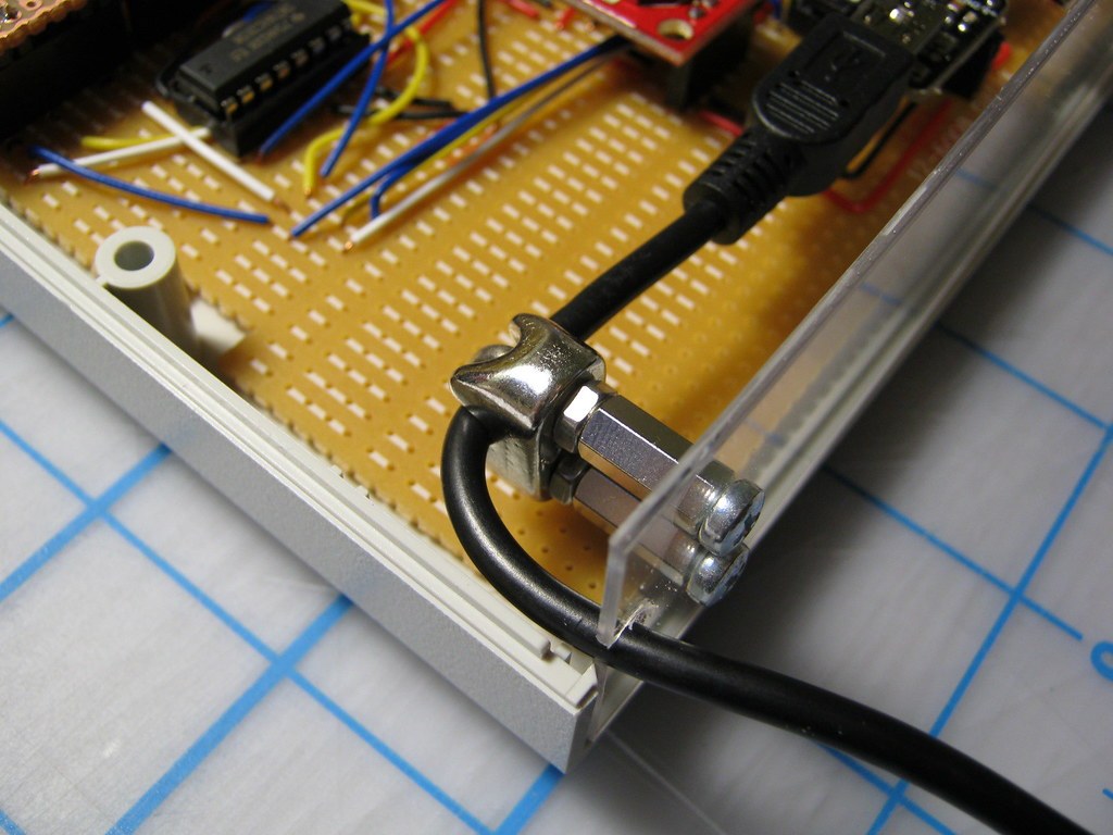
| 1 | Cable clamp | Metal cable clip on two hex stand-offs | P-clip or cable tie-down with M3 stand-off | Same | Strain relief for the USB cable |
| 1 | Cable | USB A to mini-B | USB cable to suit the adapter or Nano | Same | |
| — | Sleeving | Heat-shrink over the two thin daughter boards | Heat-shrink tubing, about 12 mm | Same | ”Extra heat-shrink short-protection slipped over the thin daughter boards” |
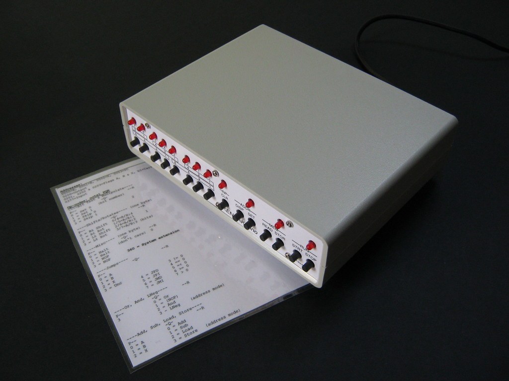
| 1 | Cheat sheet | Laminated card: op-codes on one side, extensions on the other | Print cheatsheet.html from the repository and laminate | Same | Wilson’s card is in the repository |
The firmware is the one part that costs nothing. It is under the MIT licence; the repository also carries the cheat sheet, the faceplate PostScript is on Wilson’s own site (funnypolynomial.com), and the series’ simulator and serial tool (Volume 13) work with it unchanged.
15.6 Building It
Wilson’s photographs follow the build in order, and the copy below follows them.
15.6.1 The front panel: two boards squeezed together
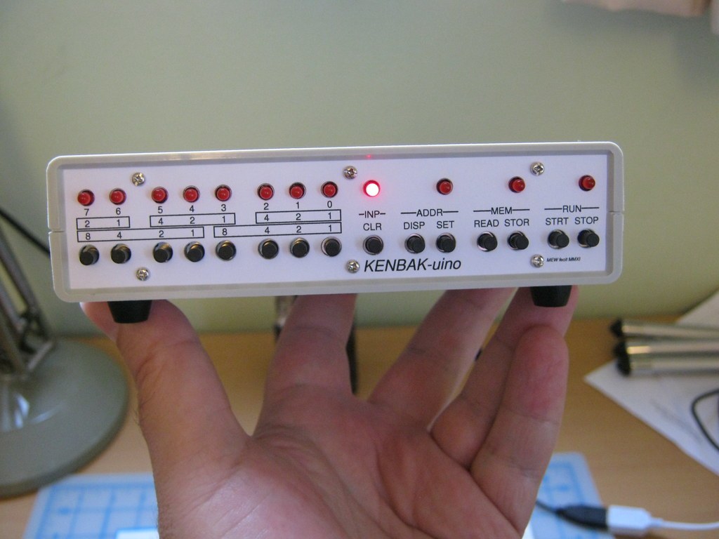
The front panel is the hard part, because the KENBAK’s proportions put the lamps and buttons close together: in Wilson’s layout every lamp and button sits on a 0.1 in grid, and the pairs that the original groups (bits 7–6, 5–4–3, 2–1–0) are only three grid squares apart. His solution was a stack of two thin boards. “To keep the proportions right, the LEDs and buttons needed to be quite close so I ended up with parallel daughter boards” (Flickr, “The Front Panel — Back”).
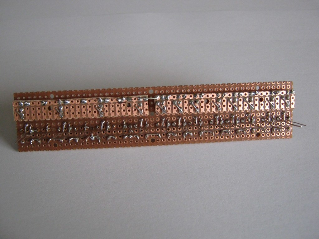
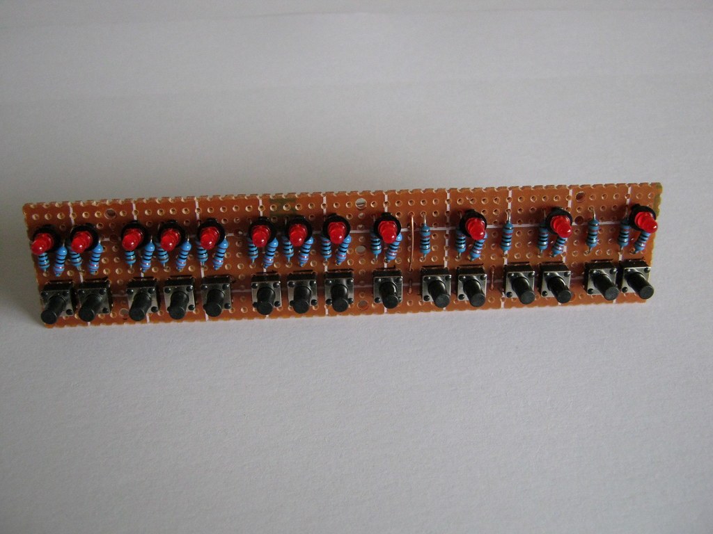
- Board 1, the panel. A strip of perfboard about the width of the faceplate carries the twelve LEDs and fifteen buttons on the faceplate’s grid, with the lamp and pull-down resistors behind them. The faceplate’s own drilling guide (below) is the template: tape it to the perfboard and the holes line up with the board’s 0.1 in pitch.
- Long legs as connectors. “To keep things simple, I preserved long resistor legs as connectors out the back” (Flickr, “The Front Panel — Daughter Board”). Each lamp or button signal leaves board 1 on the uncut leg of its resistor.
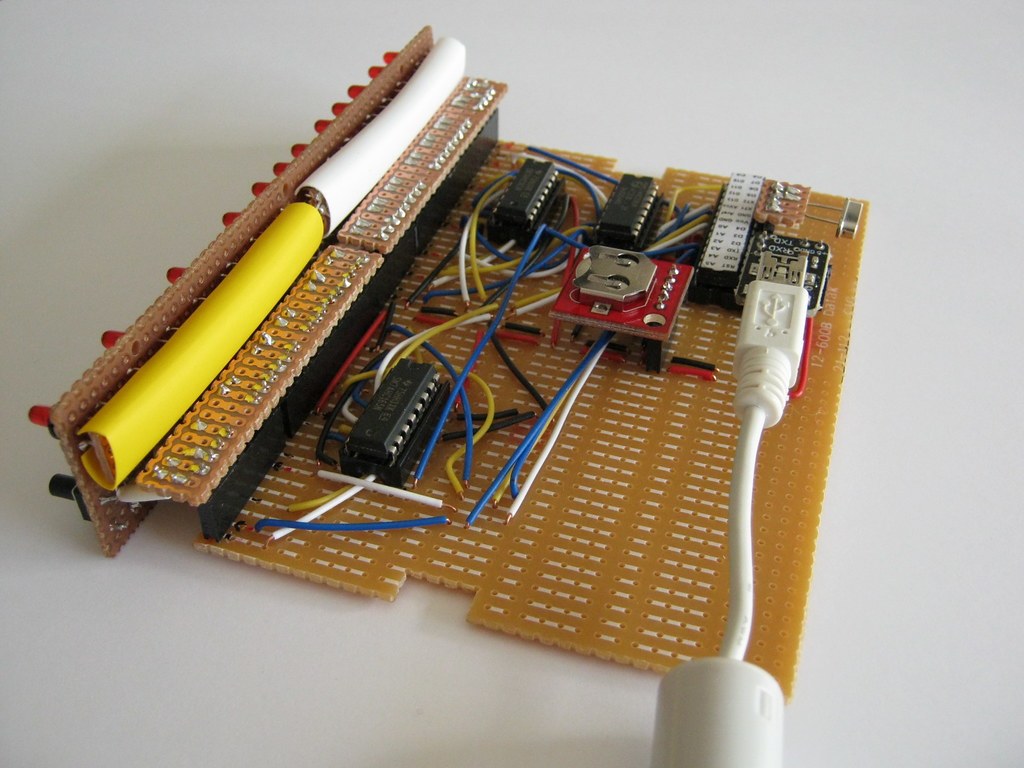
- Board 2, the spreader. The legs pass through a second, parallel strip a few millimetres behind, which gathers them onto a row of header pins along its lower edge. Its header pins point down, at right angles to the panel, and plug into a socket strip along the front edge of the main board.
- Insulate. The two thin boards sit with their solder sides close together, so a sleeve of heat-shrink goes over the pair.
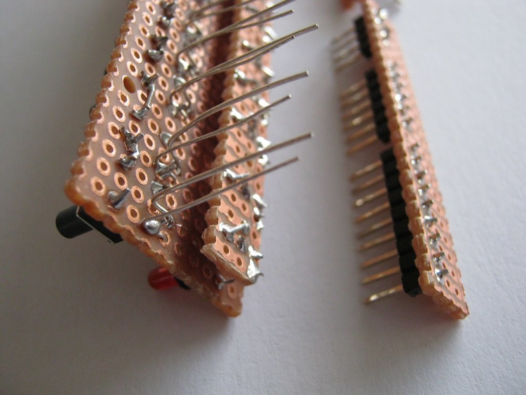
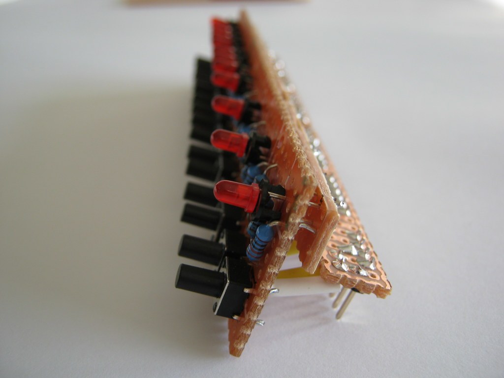

A builder who would rather not hand-wire 27 panel parts on two strips has two simpler routes. The first is a single small printed circuit board for the panel, drawn on the faceplate grid; a 135 × 31 mm two-layer board is a cheap order from any board house. The second is a ribbon cable from board 1 to the main board instead of the second strip, at the cost of a less tidy inside.
15.6.2 The main board
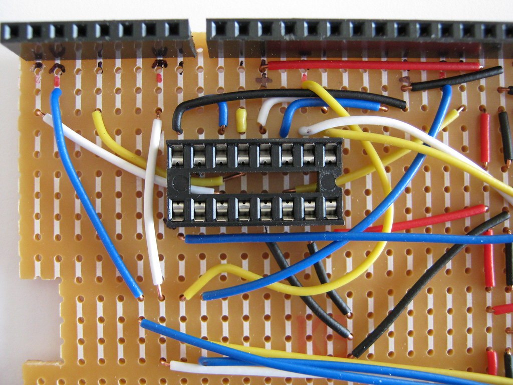
The main board is a rectangle of perfboard with notches cut in its edges where the case’s moulded posts and card guides are. “Cut-outs in the main board to accomodate the enclosure” (Flickr, “Perspective”). Wilson describes the layout of the empty board: a “header strip for the front panel along the top”, above it two sockets for the 74HC165s, “the socket for the single 74HC595 controlling 8 LEDs … below that”, “a header strip for the DS1307 RTC with the ATMega socket next to it”, and a T-shaped header “for the power supply and crystal”. Between them: “Crazy point-to-point wiring (with a sadly limited palette of colours)” (Flickr, “The Main Board — Unpopulated”).
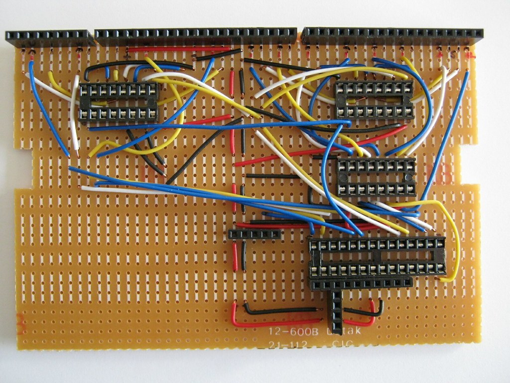
The wiring follows the schematic, and it is worth doing in this order, testing as each group is finished:
- Power. Run +5 V and ground to every socket’s supply pins (ATmega pins 7, 20 and 8, 22; each ‘595 and ‘165 pins 16 and 8) and fit the decoupling capacitors. Before any chip is in, power the board from USB and check 5 V at every socket.
- Processor. Crystal and load capacitors, reset pull-up and auto-reset capacitor, the adapter header (TX to RX, RX to TX). With only the ATmega in, a “Blink” sketch on pin 13 proves the chip, its clock and the upload path.
- Lamps. The ‘595 and its three control lines (D8, D9, D10) to the panel header; the four direct lines (A1, A2, A3, D11).
- Buttons. Both ‘165s: PL and CP from D12 and D13 to both chips, chip #2’s Q7 into chip #1’s DS, chip #1’s Q7 to A0, CE (pin 15) and the spare input to ground.
- Clock. The module’s four pins to A4, A5, 5 V and ground.
One of Wilson’s notes on the wiring is a small trick for perfboard: “To slightly simplify all those wires, I came in under some sockets, rather than looping around the back” (Flickr, “Socket Closeup”), that is, he ran wires across the board beneath the sockets before plugging the sockets in.
With an Arduino Nano the main board is simpler: a Nano on two rows of socket strip replaces the ATmega socket, the crystal header, the reset parts and the USB adapter, and its USB socket faces the rear panel. Wire D8–D13 and A0–A5 exactly as above; take 5 V and ground from the Nano’s 5V and GND pins. The rest is unchanged.
15.6.3 The faceplate
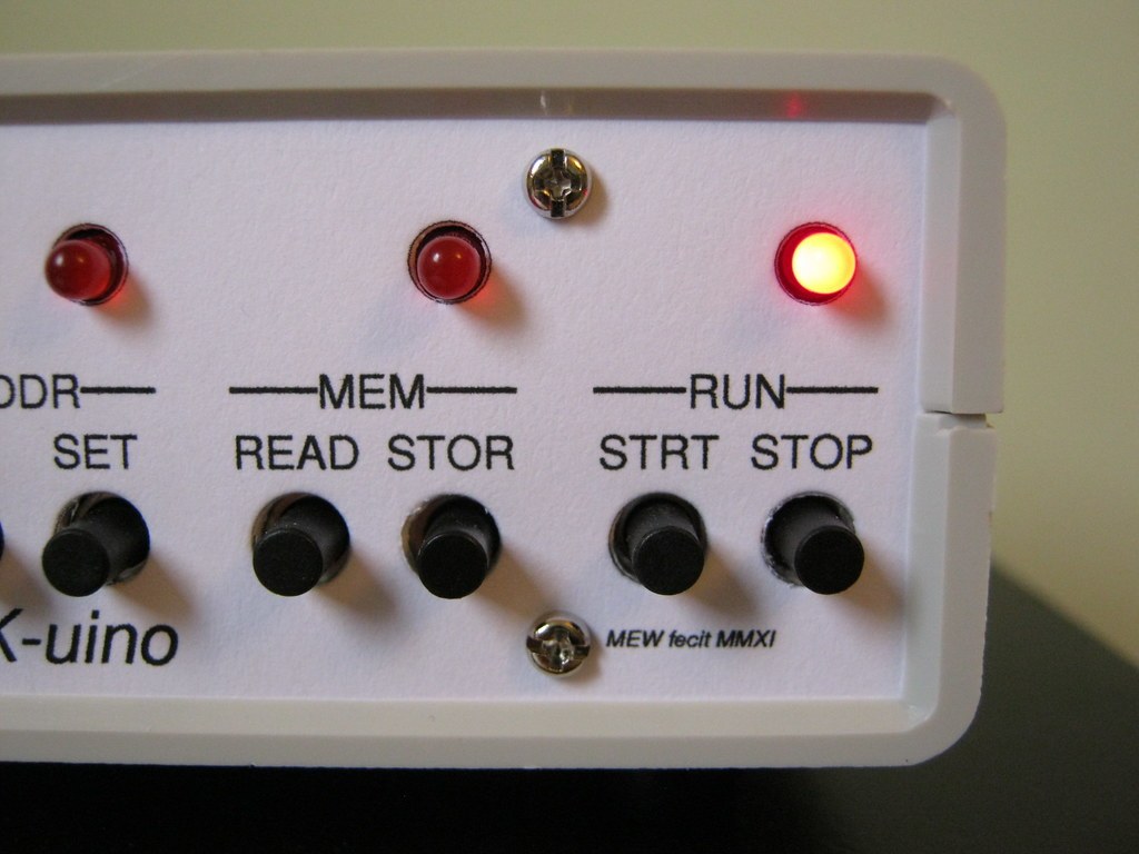
Wilson drew the faceplate in PostScript, “of course”, printed it “on fairly heavy paper then the holes punched out”, and abbreviated the KENBAK-1’s labels to fit: CLR, DISP, SET, READ, STOR, STRT, STOP (Flickr, “Faceplate”). The card sits on a plastic backing plate “drilled with my specially acquired drill-press”. The file is on his website as kenbak.ps; printed at 100 % it is full size.
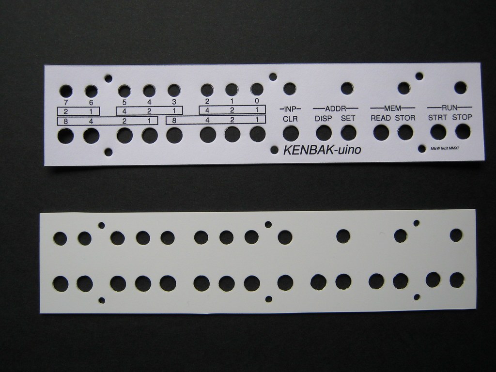
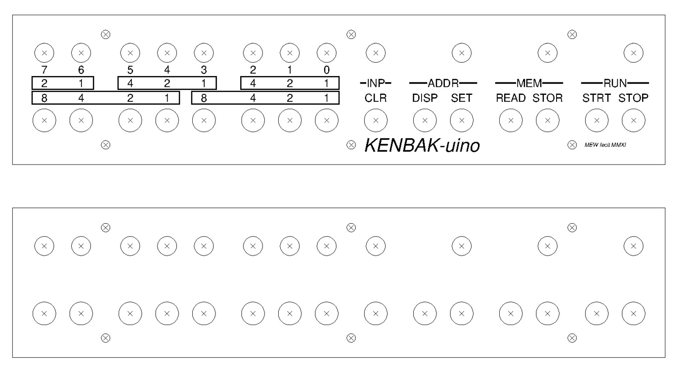
The geometry, read from the PostScript, is simple enough to lay out by hand or in any CAD program. All positions are on a 0.1 in (2.54 mm) grid; measurements are from the lower-left corner of the 135 × 31 mm frame.
Table 7 — The faceplate
| Feature | Hole | Position |
|---|---|---|
| Buttons, bits 7 → 0 | 3/16 in (4.8 mm) | 9.2 mm up; across at 6.5, 14.2, 24.3, 31.9, 39.6, 49.7, 57.3, 65.0 mm |
| Buttons, CLR, DISP, SET, READ, STOR, STRT, STOP | 3/16 in (4.8 mm) | 9.2 mm up; across at 75.1, 85.3, 92.9, 103.1, 110.7, 120.8, 128.5 mm |
| Data lamps 7 → 0 | 5/32 in (4.0 mm) | 23.1 mm up; directly above the eight data buttons |
| Control lamps INP, ADDR, MEM, RUN | 5/32 in (4.0 mm) | 23.1 mm up; above CLR, SET, STOR and STOP |
| Screws | as the screws chosen | 4.1 and 26.9 mm up; across at 19.2, 70.0 and 115.8 mm |
The spacing inside each group is 3 grid squares (7.6 mm), with 4 squares between groups. That is the KENBAK-1’s grouping in octal digits: two bits, three bits, three bits.
A more durable faceplate than paper is easy to have. The artwork can go to a sign shop for printing on adhesive vinyl, or be laser-engraved on anodised aluminium; or the legend can be printed mirror-image on the back of clear acrylic, which is what Wilson’s file anticipates. The backing plate is drilled from the bottom half of the figure, taped on as a template.
15.6.4 Into the case
“The boards socketed together and the faceplate bolted to the board and slotted into the enclosure” (Flickr, “Assembled — Front”). The faceplate screws pass through into the front-panel board, so the panel, the boards and the faceplate are one unit that slides into the case’s front slot, and the main board rides in the card guides.
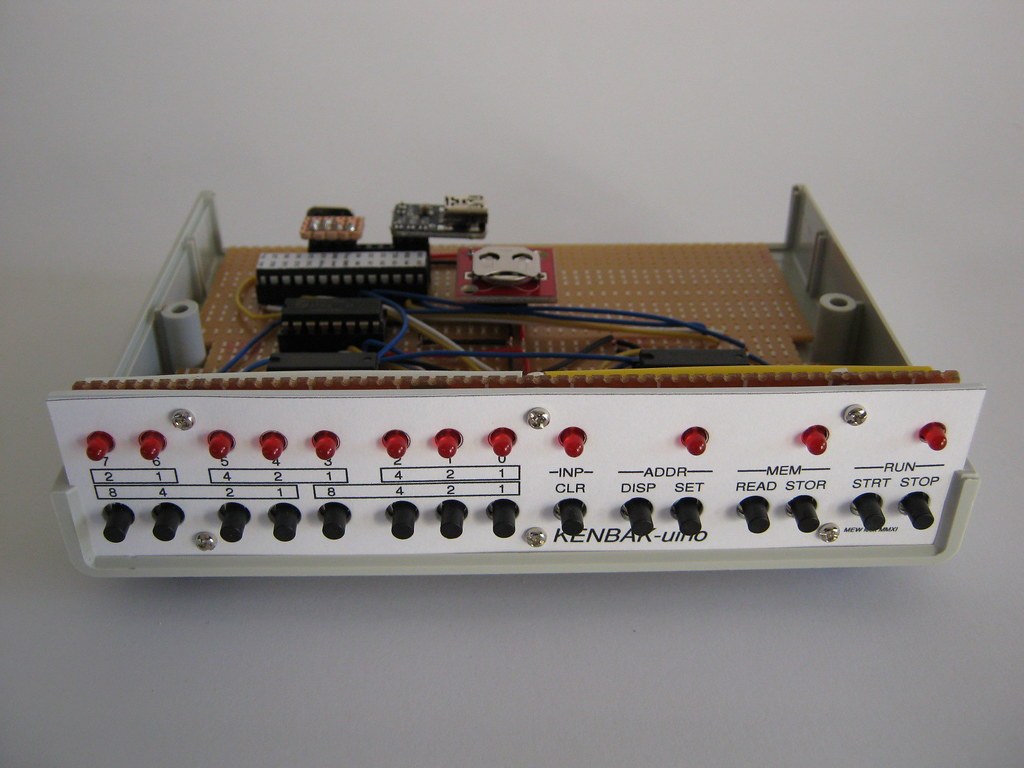
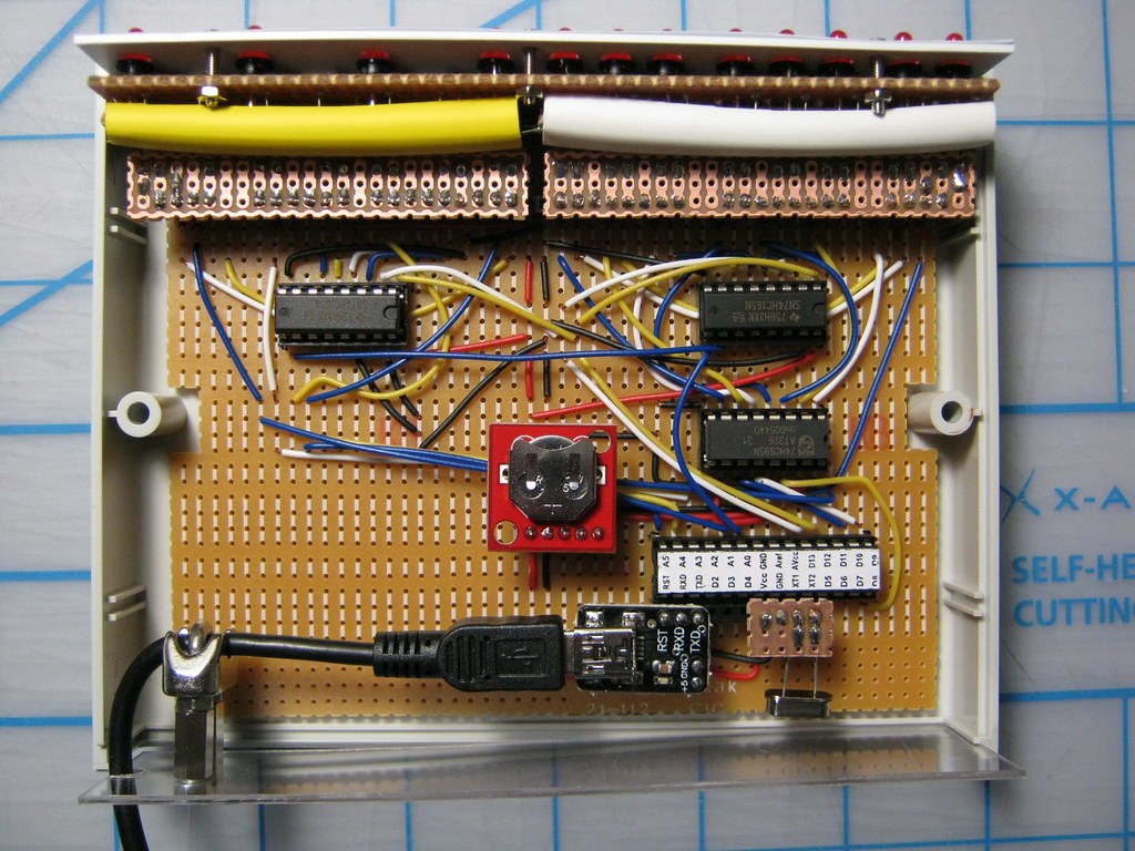
The USB cable is held by a metal cable clip on two hex stand-offs screwed through the rear panel, so a tug on the cable does not reach the small connector on the adapter board (Flickr, “Strain Relief”). With a Nano, the same clamp is even more worth having, because the Nano’s own USB socket is all that holds the cable.
15.7 Loading the Firmware
The sketch is plain Arduino code with no libraries beyond the two that come with the Arduino software, Wire (for the clock) and EEPROM. Volume 13 gives the full procedure for rebuilding it, command-line and in-system-programmer routes included; for a KENBAK-uino the short version is:
- Download the repository from GitHub. If it unpacks as
Kenbakuino-master, rename the folderKenbakuino, because the Arduino software insists that the folder match the sketch’s name (README). - Choose the clock. For a DS1307 module, change nothing. For a DS3231, set the three constants near line 16 of
Clock.hto0x68,0x0E,0x00. For no clock at all, setRTC_I2C_ADDRto0x00; the clocks will not keep time, but everything else works and the settings go to EEPROM. - Choose the board. For a bare ATmega328P with the Uno bootloader, the board is “Arduino Uno”; the USB adapter’s reset line restarts the chip for the upload. For a Nano, “Arduino Nano”, and on most clone Nanos the processor option “ATmega328P (Old Bootloader)”.
- Upload, then open a serial monitor at 38,400 baud: that is the firmware’s speed (
Serial.begin(38400)inKenbakuino.ino).
Three switches in the code select older behaviour, for anyone who wants Wilson’s machine exactly as it was in 2011: CPU_LEGACY_SHIFT_ROLL and CPU_LEGACY_PROGRAM_COUNTER in CPU.cpp, and MCP_LEGACY_RUN_LED in MCP.cpp, all commented out by default. Leaving them off gives the corrected emulation that Volumes 6, 7 and 10 assume.
Setting the clock. Built-in program 7, “Set RTC”, sets the time from the A and B registers: hours in A and minutes in B, both in binary-coded decimal, 24-hour (kenbakuino.txt). Load it with Stop + Bit 7; store the hours at address 000 and the minutes at 001 (for 14:35, 024 and 065 in octal, which are 0x14 and 0x35); press Start.
15.8 First Power-Up and Testing
A short sequence finds every wiring fault in the panel. It uses only the firmware’s own front-panel behaviour, so it needs no test program.
- Supply. With no chips in their sockets, 5 V on every socket’s supply pin, and no more than a few milliamps drawn.
- Lamps. Chips in, power on. Press a data button: in the firmware’s default mode each press toggles that bit, and its lamp should follow. Light each of the eight in turn; a lamp lighting in the wrong place means its ‘595 output is wired out of order (or the shift direction does not match the wiring).
- Buttons. Each button should act on its own bit or function. If pressing bit 2 lights bit 6, the button wiring and
m_pMap[]disagree; correct one or the other. - Control buttons. CLR clears the eight lamps; DISP shows the address; SET makes the displayed value the address; READ and STOR read and write memory, and STOR advances the address.
- Run. Load built-in program 1 with Stop + Bit 1 and press Start. Without a slow-down it is a blur; Bit 3 + Stop slows it to 8 ms per instruction, and a single lamp sweeps left and right across the eight. That exercises the lamps, the RUN lamp and the processor together.
- Clock. Load built-in program 4 (the binary clock) with Stop + Bit 4 and Start: the minutes appear on the data lamps with the leftmost one blinking, the hours on the control lamps. If nothing advances, check the I²C lines and the
Clock.hsetting against the module fitted. - Emulation. Key in Volume 9’s acceptance program. It finishes in ten instructions with alternate lamps lit (252) on a current build.
15.9 Programming It
15.9.1 The program in Wilson’s video
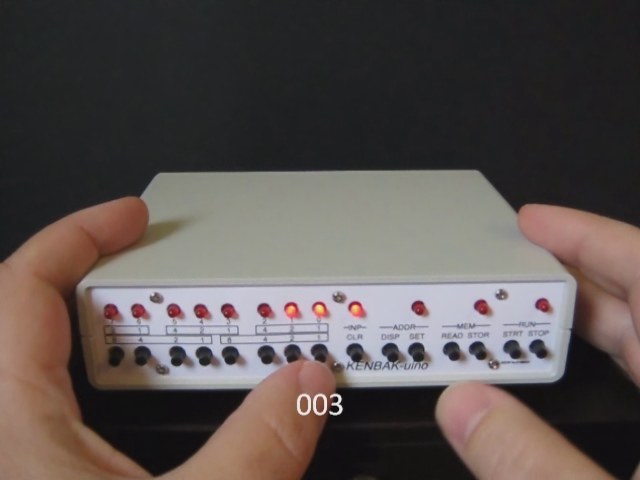
Wilson’s Flickr set includes a short silent video, “Programming the KENBAK-uino”, in which he keys a counting program by hand and runs it (Flickr). It is the KENBAK-1’s first program in miniature: add one, show it, repeat. It is also, byte for byte, the firmware’s built-in program 0, the “Simple counter” that Stop + Bit 0 loads (programCounter[] in Memory.cpp).
As it runs in the series’ simulator (03-outputs/tools/vol15_programs.py, which keys it on the simulated panel exactly as below):
Loc  Contents  Symbolic
003  004       P: start at 004
004  103 001   ADD B C=001      add 1 to B
006  134 200   STORE B 200      show B in the lamps (OUTPUT)
010  344 004   JPD UNC 004      and again
Wilson’s caption calls 103 “the ‘ADD constant to register A’ op-code”, but the instruction’s top two bits, 01, select register B, and 134 likewise stores B (Volume 6 sets out the instruction fields). The program is right; only the caption’s letter is wrong, and since nothing else touches B, the program counts either way.
To key it, the way the video does:
- Clear, enter 003 on the data buttons, Set: the address is now 003.
- Clear, enter 004, Store: P is set to 004, and Store moves the address on to 004.
- For each of 103, 001, 134, 200, 344, 004: Clear, enter the byte, Store.
- Start.
On the KENBAK-uino the data buttons toggle by default, which is why the video sometimes clears before entering a byte and sometimes edits the one already showing.
Run at full speed, the lamps are a blur. Wilson’s answer is the firmware’s speed extension: he stops it, presses Bit 4 + Stop, which adds 2⁴ = 16 ms after every instruction, and starts it again. The loop is three instructions, so each count then takes at least 48 ms: about twenty counts a second, slow enough to see the binary count ripple across the lamps. In the simulator, thirty instructions after Start the lamps show ○○ ○○● ○●○ (012), ten passes of the loop, and after 256 counts the byte wraps to 000 and carries on.
The original KENBAK-1, at a few hundred instructions a second (Volume 3), needed no slowing down. Volume 7 gives a version of this program with a delay loop, which runs at a watchable speed without any extension.
15.9.2 The extensions
Everything Volume 9 lists for the µKENBAK-1 is Wilson’s, and works the same on a KENBAK-uino: each is two buttons pressed together while the program is stopped, the first held down (kenbakuino.txt).
Table 8 — The extensions
| Keys | Does |
|---|---|
| Stop + Bit N | Load built-in program N: 0 counter, 1 pattern, 2 counting clock, 3 BCD clock, 4 binary clock, 5 “Das Blinken Lights”, 6 Sieve of Eratosthenes, 7 set the clock |
| Bit N + Stop | Slow the processor: 2ᴺ ms after each instruction |
| Clear + Store | Erase memory; P = 004, address 004 |
| Stop + Clear | Blank the lamps |
| Bit N + Store / Bit N + Read | Save memory to / load it from EEPROM page N |
| Bit N + Display / Bit N + Set | Send memory to / receive it from the serial port; N sets 4,800–38,400 baud |
| Stop + Read / Stop + Store | Read / write a system setting from the front panel |
| Hold Stop + Bit N (or Read + Bit N) at power-on | Run built-in program N (or EEPROM page N) every time it is switched on |
Programs can also call the firmware directly with the op-code 360, which Wilson took from the KENBAK-1’s unused two-byte no-operation codes: A selects the function and B carries the value. That reads the clock, a random number, the serial port, and controls the lamps and EEPROM. Programs that use it do not run on an original KENBAK-1 or in the series’ simulator, which treats 360 as the no-operation it was in 1971. Volume 13 has the full list and a worked clock program.
15.9.3 Loading programs over USB
Typing programs into a computer and sending them is the extension that changes the machine most, and it is the same on the KENBAK-uino as on the kits: Bit N + Set to receive, Bit N + Display to send, octal numbers separated by commas and ended with s, and a reply giving the length and checksum. Volume 13 covers it in detail, and the series’ tool ukenbak_serial.py, despite its name, works with any machine running Wilson’s firmware.
15.9.4 A pattern for the lamps
Built-in program 1 is the “Cylon” sweep of the testing section, one lamp bouncing from end to end. It uses no extensions, so it runs on an original KENBAK-1 too. As listed in Memory.cpp and run in the simulator:
Loc  Contents  Symbolic
003  004       P: start at 004
004  023 001   LOAD A C=001     one lamp, at the right
006  034 200   STORE A 200
010  211       SFTL A 1         move it left
011  034 200   STORE A 200
013  372 200   SKP1 7 200       reached bit 7?  then skip
015  343 010   JPD UNC 010      no: keep going left
017  011       SFTR A 1         move it right
020  323 177   AND C=177        clear the copied sign bit
022  034 200   STORE A 200
024  202 200   SKP0 0 200       not yet at bit 0?  then skip
026  343 010   JPD UNC 010      at bit 0: turn round
030  343 017   JPD UNC 017      keep going right
In the simulator the lamps step 001, 002, 004, 010, 020, 040, 100, 200, then 100, 040 and so on back to 001, and turn again. The AND 177 after the right shift is the trace of Wilson’s 2021 correction: the original’s right shift copies the top bit, so 200 shifted right becomes 300, not 100, and the program has to clear it, as his comment in the source notes.
15.10 What a Copy Can Change
The KENBAK-uino is a design to copy loosely as much as exactly. The choices that matter, in the order a builder meets them:
- Bare chip or Nano. The bare ATmega328P is Wilson’s way and makes the main board look like the 2011 original; the Nano saves a dozen parts and the upload wiring.
- DS1307 or DS3231. The DS1307 runs the published code unchanged; the DS3231 keeps better time and makes the machine identical in software to the commercial kits.
- Lamp resistors. Larger values than Wilson’s 220 Ω keep the 74HC595 inside its data sheet (see the parts list).
- Button wiring. Any order the board makes easy, with
m_pMap[]edited to match. - Toggles. A power switch is easy to add; the lock key would need a spare input and a change to the firmware, as early µKENBAK-1 firmware read on pin D7 before later builds dropped it (Volume 13).
- Faceplate. Paper and punched holes, as Wilson made it, or vinyl, engraved aluminium or reverse-printed acrylic from the same artwork.
- Scale. Wilson’s machine is a little over a quarter of the KENBAK-1’s 489 mm width. The same circuit and firmware drive any panel, and Adwater & Stir’s half-scale µKENBAK-1 and Volumes 11 and 12’s full-size case are the same idea at larger sizes.
15.11 Printable Bill of Materials
The whole parts list above is also a printable PDF for the bench: KENBAK-uino BOM (PDF). Each part has a row with tick boxes for ordered, in hand and fitted, the quantity and where it goes, the part number to buy, alternates (the one obsolete part names its replacement), where to buy it, its tag and space for notes. The last page is an order log.
Back to the start — Volume 1: KENBAK-1 — The First Personal Computer. From a pocket-sized grey box back to the blue machine that started it: John Blankenbaker’s 1971 computer of lights and switches, its advertisement in Scientific American, and the museum contest that named it the first personal computer.
Comments (0)