KENBAK-1 · Volume 3
KENBAK-1 — Volume 3 — A Computer Without a Microprocessor — TTL and Shift-Register Memory
How 130-odd catalogue logic chips, two 1,024-bit MOS shift registers and a 29-state controller made a stored-program computer in 1971: why it works one bit at a time, why its registers live in memory, why a byte can only be read when it comes round, and what that cost in speed
3.1 About This Volume
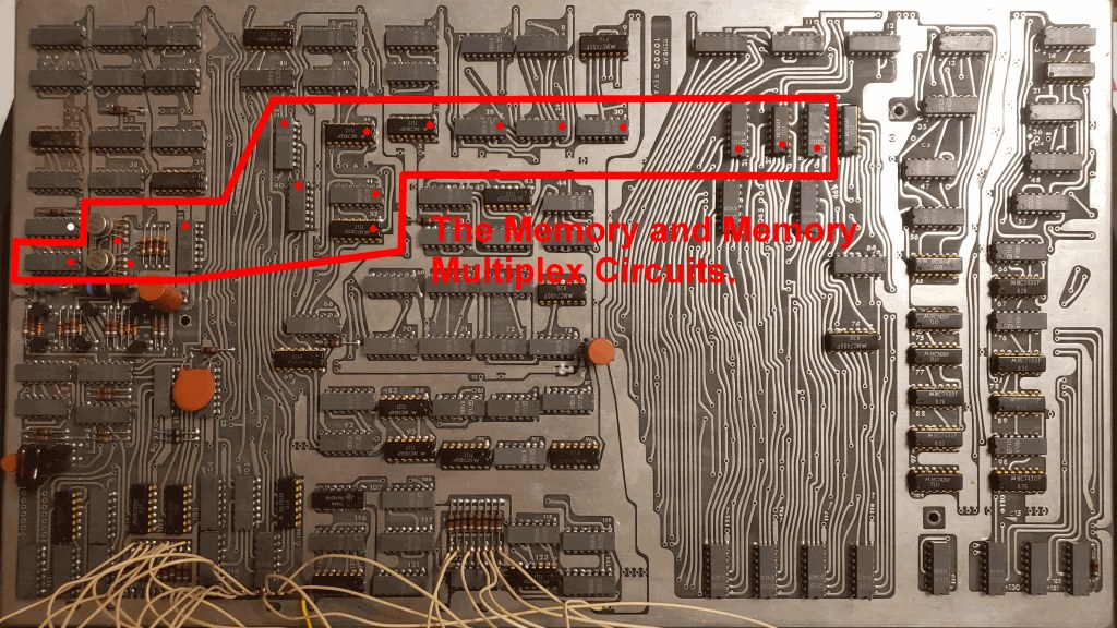
The KENBAK-1 was designed in the last months of 1970 and the first months of 1971, and it went on sale in the autumn of 1971. The Intel 4004, the first microprocessor offered on the open market, was announced in Electronic News on 15 November 1971 (Computer History Museum, “This Day in History”, 15 November). There was therefore no processor chip that John Blankenbaker could have bought, and the machine has none. Its “processor” is a printed circuit board of about 130 ordinary logic chips from the Texas Instruments 7400 family and its second sources, and its memory is two shift-register chips made by Intel.
This volume takes that board apart. It explains the parts Blankenbaker chose and why, then the three design decisions that follow from them: the machine is serial, handling one bit at a time; its programming registers are not hardware registers but bytes in memory; and its memory is sequential, a loop of bits that can only be read as it passes. It closes with the cost of those decisions in speed, estimated with the series’ own timing model, and with a short account of the power supply, lamps and switches.
The main sources are Kenbak Corporation’s own Theory of Operation manual (1971), which gives the block diagram, state diagram and complete logic schematics, and the Programming Reference Manual dated 4/1/71. Scans of both are online at Adwater & Stir (originally from Grant Stockly’s kenbakkit.com). Blankenbaker’s own words come from a talk he gave at The Computer Museum in Boston in 1986, transcribed by the Computer History Museum (Chris Garcia, “In His Own Words: John Blankenbaker”, CHM blog, 5 April 2016). Volume 1 places the machine in its history, Volume 2 tells Blankenbaker’s story, and Volume 6 describes the instruction set that this hardware carries out.
3.2 1971: Building a Computer From a Parts Catalogue
3.2.1 What was on the shelf
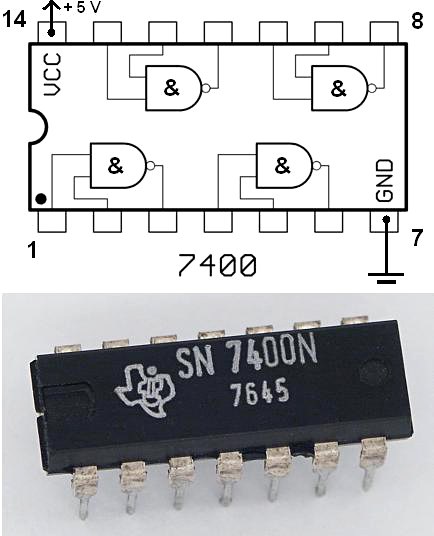
By 1970 a designer who wanted to build a small digital machine had two cheap commodities to work with. The first was transistor-transistor logic (TTL). James Buie of TRW patented the TTL circuit in 1961; Sylvania brought out the first TTL family, SUHL, in 1963; Texas Instruments answered with its SN5400 military series in 1964 and, in 1966, the SN7400 series “in low cost plastic packages for industrial customers”, which quickly took more than half the logic market (CHM Silicon Engine, “1963: Standard Logic IC Families Introduced”). A 7400 chip holds four two-input NAND gates; a 7474 holds two flip-flops. By 1970 parts like these were made by Texas Instruments, Motorola, National, Fairchild, Signetics and others, all to the same numbers and pin-outs, and they cost cents to a dollar or so each.
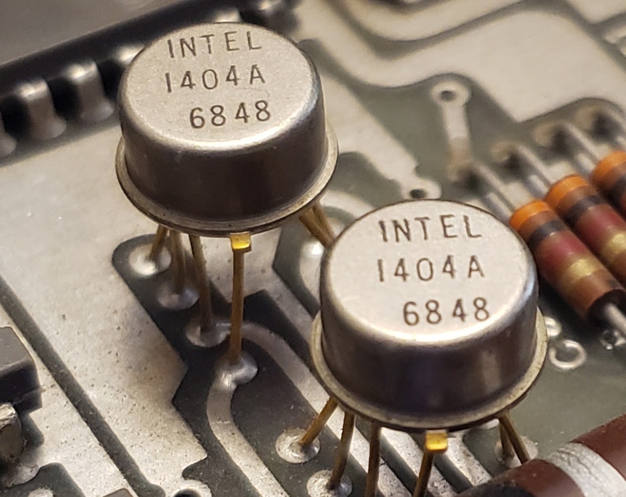
The second commodity was new: MOS memory. Intel, founded in 1968, sold its first products in 1969 and 1970. Some were random-access memories; others were shift registers, long chains of storage cells through which bits march one step per clock pulse. A shift register needs no address decoding and few pins, so it could be made denser and cheaper than random-access memory of the same era; its drawback is that a given bit can only be read when it reaches the end of the chain (Ken Shirriff, “Inside the Intel 1405: die photos of a shift register memory from 1970”, righto.com, December 2014). Datapoint’s 2200 terminal of 1970 used Intel shift registers both for its main memory and for its screen.
What did not exist was a single chip that fetched and executed instructions. Building a computer in 1970 meant building that part out of gates.
3.2.2 Blankenbaker’s rules for parts
Blankenbaker had been thinking about small computers since the 1950s. In 1958 he published a design for a computer controlled by the program stored in its own memory, with almost no fixed logic (“Logically Micro-Programmed Computers”, IRE Transactions on Electronic Computers EC-7, no. 2, June 1958, pp. 103–109). He reported in a 2021 note that the idea was that “only one logic flip flop was needed” (Blankenbaker, July 2021, reprinted in the Adwater & Stir µKENBAK-1 Assembly & Operations booklet, rev. 2.5). When he finally built a machine to sell, cost was the constraint that shaped everything. In his 1986 talk he recalled the target:
I still had the fixation upon the $500 selling price, which meant $150 perhaps of cost.
and the rule he set himself for parts:
I will choose IC’s which are most widely available from the most manufacturers and sell them at the lowest cost.
The KENBAK-1 sold for $750, not $500 (Volume 4), but the rule held. The Theory of Operation manual lists every logic type on the board: fourteen kinds of integrated circuit, all from the 7400 family, all in fourteen-lead packages except one sixteen-lead decoder. It names Motorola, National, Texas Instruments, Signetics and Fairchild as sources, “though this is not an exhaustive list”.
Table 1 — Blankenbaker's rules for parts
| Type | Function | Type | Function |
|---|---|---|---|
| 7400 | quad 2-input NAND | 7442 | BCD-to-decimal decoder |
| 7403 | quad 2-input NAND, open collector | 7451 | dual 2-wide AND-OR-INVERT |
| 7404 | hex inverter | 7454 | 4-wide AND-OR-INVERT |
| 7408 | quad 2-input AND | 7474 | dual D flip-flop |
| 7410 | triple 3-input NAND | 7486 | quad exclusive-OR |
| 7416 | hex inverter buffer, open collector | 7495 | 4-bit shift register |
| 7420 | dual 4-input NAND | 7430 | 8-input NAND |
The fourteen logic types of the KENBAK-1, from the “Definition of Logic Elements” section of the Theory of Operation manual.
How many chips that came to is given slightly differently by different sources. Blankenbaker said in 1986: “There are 130 ICs in that computer right there, but they are cheap ICs.” The kenbak.com site, working from the schematics, counts 131, of which 45 are 7400s, and notes that the state machine alone accounts for 31 (kenbak.com, “Design of the Kenbak-1”). Reproduction builders (Volume 8) work to the same figure. Add the two memory chips, a handful of transistors for the clock and the memory clock drivers, resistors, capacitors and the front-panel parts, and that is the whole computer.
3.3 Memory That Goes Round
3.3.1 From mercury to MOS
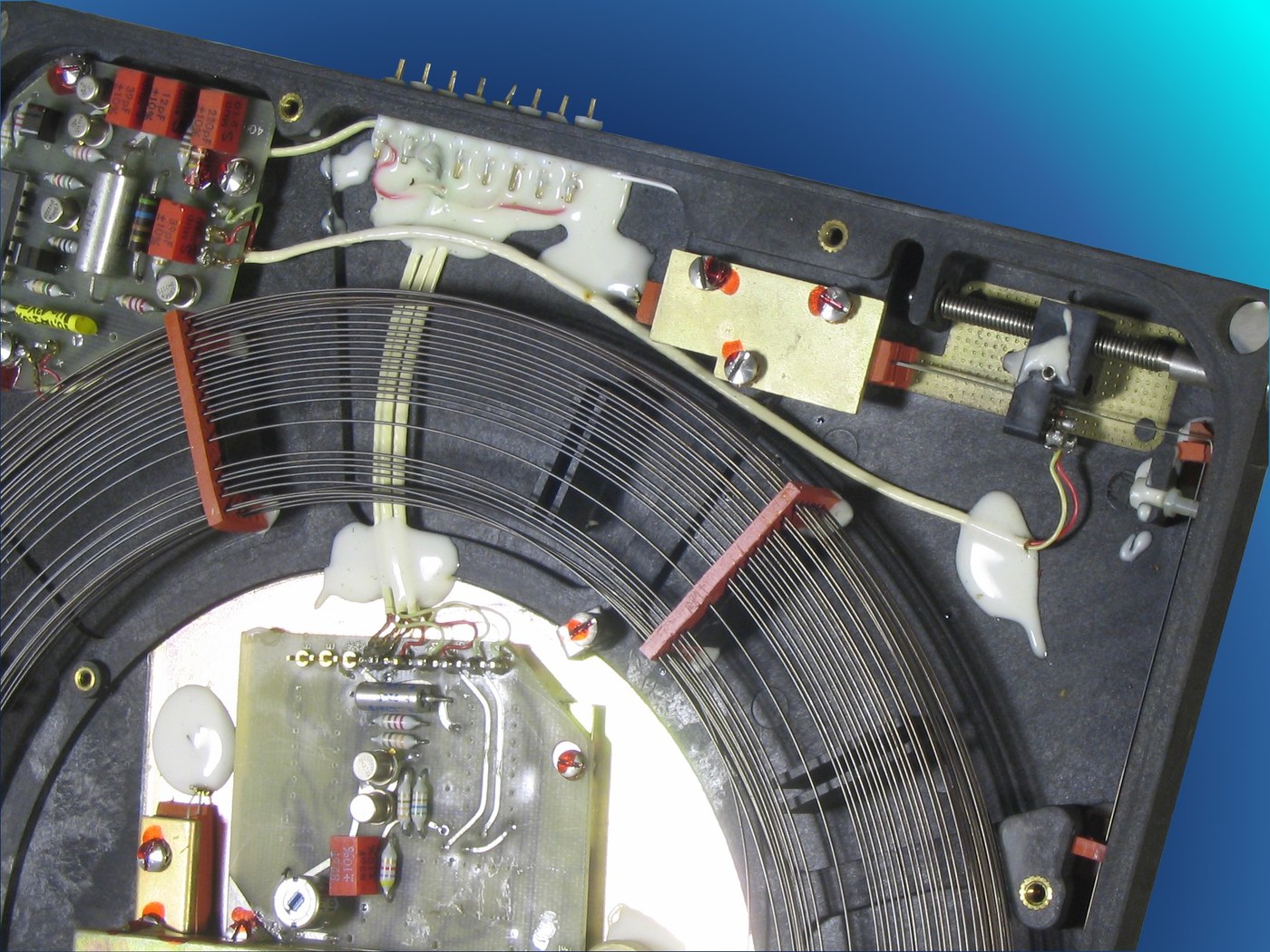
Memory that holds data by keeping it moving is as old as the stored-program computer. EDSAC in 1949 stored its words as sound pulses travelling down tubes of mercury, re-amplifying and re-injecting each pulse as it emerged; later machines used magnetostrictive delay lines, coils of nickel wire along which a torsional pulse ran for a few milliseconds. The principle never changed: the store is a loop, each bit has a time slot rather than a place, and to read a bit the machine waits for its slot to come round. The MOS shift register is the same idea in silicon: a chain of 1,024 cells, a two-phase clock that moves every bit one cell along, and the output wired back to the input so that the contents go round for as long as the clock runs.
Blankenbaker chose this deliberately. In 1986 he said: “The one most economical memory [technology] I could find was MOS shift registers.” The alternative, magnetic core, would have been, in the words of the kenbak.com account, “terribly expensive and large” for even 256 bytes.
3.3.2 The Intel 1404A
The parts are two Intel 1404A dynamic shift registers, each storing 1,024 bits in a single chain. Intel’s own data sheet for the 1404A has not been found for this volume; the Synertek data sheet for its second-source SY1402A/1403A/1404A family describes the same family — 1,024 bits organised as four chains of 256 (1402A), two of 512 (1403A) or one of 1,024 (1404A), the 1404A in an eight-lead TO can or plastic package, inputs and outputs compatible with TTL, a two-phase clock, and supplies of +5 V and −5 V or −9 V (Synertek data sheet, via bitsavers). “Dynamic” means each cell holds its bit as charge on a tiny capacitor that leaks away within milliseconds; the bits survive only because the clock keeps moving them on and the cells keep re-forming them. Stop the clock for long and the memory is lost. Turn the power off and it is certainly lost, which is why the Programming Reference Manual warns that “When power is turned on, random data will appear in the memory.”
The clock lines of these chips swing far beyond TTL levels. On the KENBAK-1 a two-transistor multivibrator generates the main clock, a small two-phase generator produces the shift-register clocks F1 and F2, and level shifters convert them to swings of about +5 to −12 volts (kenbak.com, “Design of the Kenbak-1”). The Theory of Operation manual describes the MOS shift registers as needing “two clock signals out of phase with each other. One occurs during the even bit times and the other occurs during the odd bit times.”
3.3.3 Two loops of 128 bytes
Each 1,024-bit register holds 128 bytes. In the manual’s words: “Bytes with addresses 000 to 177 (octal) are in delay line 0 and bytes with addresses 200 to 377 (octal) are in delay line 1.” (The manual calls the shift registers “delay lines” throughout, the name inherited from mercury and wire.) The two registers are clocked together, so byte 000 and byte 200 emerge at the same moment, then byte 001 and byte 201, and so on round to 177 and 377 and back to 000 and 200. “Circulation of the information within the delay lines is continuous. It never stops.”
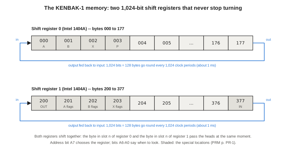
An address therefore has two parts. The top bit, A7, chooses the register; the lower seven bits say when to look. A counter called the L register counts byte times, 0 to 127 and round again, keeping track of which slot is at the heads. To read or write address a, the machine loads a into a comparator and waits until the seven low bits of the counter match; the next byte to arrive is the one it wants. The manual: “The memory address register is, in effect, one byte time ahead of the memory.” At about a million bits a second, one trip round the loop takes 1,024 bit times, about a millisecond, and the average wait for a random byte is half that.
The consequence for a programmer is simple and severe. Every access to memory — every instruction fetch, every operand, every register — costs up to a millisecond of waiting. The next section shows how the design lives with that.
3.4 Serial by Design
3.4.1 One bit at a time
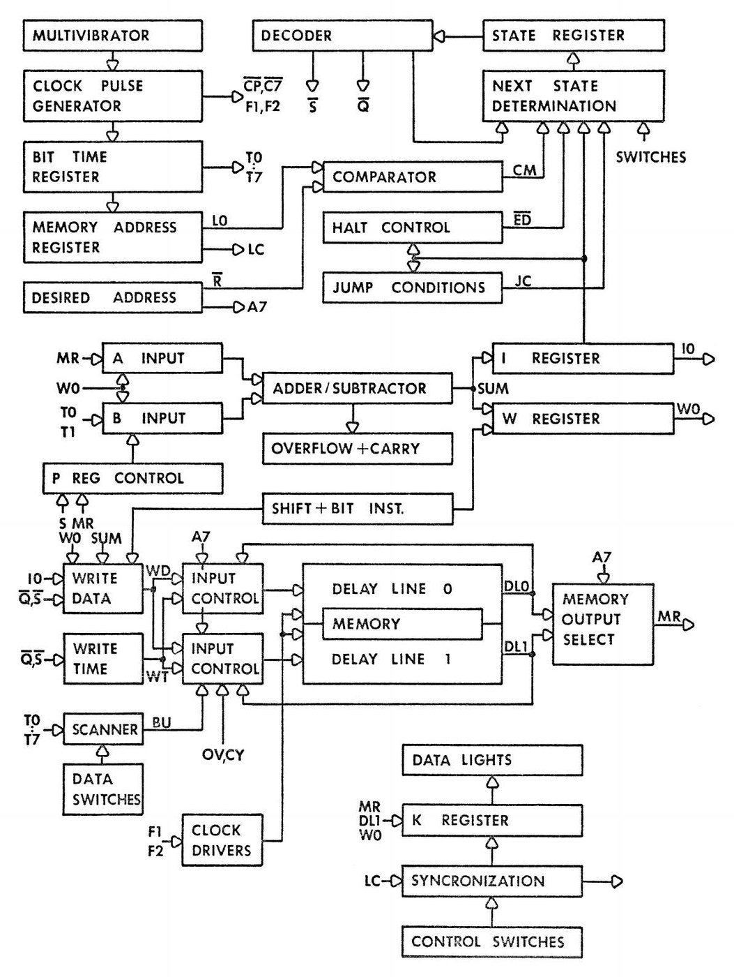
The Theory of Operation manual opens its block diagram section by saying that the KENBAK-1 “differs internally in its structure from the majority of computers in these two ways.” The first is that “The computer is serial. Data is read, or written, from the memory one bit at a time. Thus it takes eight clock times to read a byte from the memory.”
Once the memory delivers one bit per clock, there is no point in moving data any other way. The adder is a serial adder: one full-adder circuit and a carry flip-flop, fed with the two operands least-significant bit first, producing one bit of the sum per clock and remembering the carry for the next. Eight clock times make one byte time, and an eight-bit addition costs no more hardware than a one-bit addition. A clock of about 1 MHz is divided into eight bit times, T0 to T7, by a ring counter in which a single 1 circulates; T0 to T7 together are one byte time, and every state of the machine starts at a T0 and ends at a T7.
Serial arithmetic was the standard economy of early computers, and Blankenbaker had worked with it from the beginning of his career, on the National Bureau of Standards’ SEAC as a student intern and on Hughes Aircraft’s airborne machines (Volume 2). In 1971 it suited a $750 computer for the same reason it had suited a vacuum-tube one: logic was the expensive thing, and time was cheap.
3.4.2 Registers that live in memory
The manual’s second difference is the stranger one: “The programming registers (A, B, X and P) do not exist as actual hardware registers. Instead, a fewer number of hardware registers are time-shared to provide the necessary data manipulation.” The accumulator A is memory byte 000, the second accumulator B is 001, the index register X is 002, and the program counter P is 003.
Because memory is serial and must be waited for anyway, keeping the registers there costs little extra time and saves a great deal of hardware: three 8-bit registers and an 8-bit counter, each needing eight flip-flops and their gating, would have been dozens of chips. Instead the board carries two working registers:
- The I register holds the first byte of the current instruction. It is also used to hold data being stored into memory and for the front-panel operations.
- The W register is “a general purpose working register which holds data, addresses and operands”. It is where the second byte of an instruction goes, where an indirect or indexed address is built up, and where shifts and rotates actually happen.
There is a programming bonus, which Blankenbaker valued as a teacher. Because the registers have addresses, every instruction that works on memory also works on the registers. “SUB A A” clears A; “LOAD A B” copies B into A; “ADD A A” doubles A; “STORE A P” is a computed jump; “LOAD A (A)” uses A as a pointer. The Programming Reference Manual lists these “register-to-register operations” as special cases rather than separate instructions (Volume 6).
3.4.3 Why the flags are at 201, 202 and 203
The overflow and carry bits for A, B and X are kept in memory too, at addresses 201, 202 and 203. The reason for those odd-looking addresses is in the timing. An addition to A happens during the byte time when A itself, address 000, is passing through the adder — state SN in the manual. The overflow and carry are only known when the last bit has been added, at the end of that byte time. The Theory of Operation glossary defines a signal TS as “True for the byte time after SN in addition and subtraction. Controls writing of OV and CY.” The byte that comes along in the very next byte time is slot 1; in delay line 1, slot 1 is address 201. In the same way B’s flags land at 202 and X’s at 203, each one byte after its register. The manual adds that the flags are written into delay line 1 directly “through delay line 1 input control”, the same path the data switches use to write the input byte at 377.
The output byte, 200, shares slot 0 with A; the input byte, 377, is the last slot of delay line 1. The memory map that Volume 6 presents as a list of conventions is, underneath, a map of when things pass the heads.
3.5 The Control: A 29-State Machine
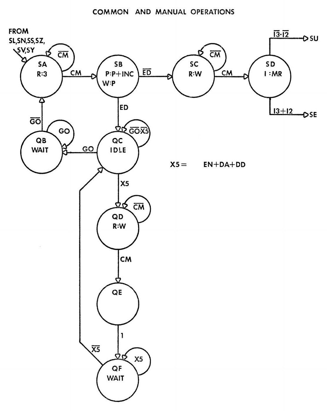
What makes this pile of gates a computer is the control, and the KENBAK-1’s control is a finite-state machine built from five flip-flops. Five bits give 32 combinations; the manual says the computer “has 29 valid states and 3 invalid states. Should an invalid state occur, which it shouldn’t except when power is turned on, a valid state is generated next.” Decoders turn the five bits into thirty-two lines, of which exactly one is active: the current state. The states are named with two letters: those beginning with S are the automatic, running states; those beginning with Q are the manual, front-panel states.
3.5.1 One instruction, state by state
The manual walks through the states in order, and they read like a recipe for running a computer out of a circulating memory. For a two-byte instruction such as “ADD B C=001” (add the constant 1 to B):
- SA — seek the P register. The desired address is 003. “If, during T7, the comparison signal, CM, is false, state SA will be regenerated for another byte time.” The machine simply waits for byte 003 to arrive.
- SB — read and update P, one byte time. The value read is the address of the instruction just finished; the circuit adds 1, 2 or 4 to it, depending on how long that instruction was and whether it skipped, writes it back and copies it into W. (This is why, in Volume 6, storing a number n into P sends the program to n + 2: the increment for the storing instruction is added afterwards.)
- SC — seek the instruction at the address now in W.
- SD — read the first byte into the I register.
- SE — read the second byte into W. It is the very next byte, so no wait is needed.
- Then, depending on the addressing mode, seek an indirect address (SF, SG), seek X and add it in (SH, SJ), and seek and read the operand (SK, SL).
- SM — seek the register named in the instruction, here B at 001.
- SN — the register passes through the adder with W, and the sum goes back in its place. The next byte time writes the flags at 202.
Stores add states to seek the destination and write it (SP, SR, SS); jumps evaluate the condition while the register passes (SZ) and then seek P to write the target (ST, SN); jump-and-mark also writes the return address (SQ, SR, SS); the one-byte shifts read A or B, shift W in a byte time, and seek A or B again to write it back (SU–SY). Every “seek” is a wait for the memory to come round.
3.6 How Fast Was It?
The Wikipedia article on the KENBAK-1 gives its speed as averaging “below 1,000 instructions per second”. No published measurement of instruction times has been found for this volume. The series’ simulator, kenbak_sim.py, therefore includes a timing model that walks the state sequence just described: each seek state lasts from one to 128 byte times, until the wanted slot is next at the heads; each working state lasts one byte time; a byte time is 8 microseconds at 1 MHz. The model is derived from the manual’s state descriptions, not measured on a machine, and its figures are estimates.
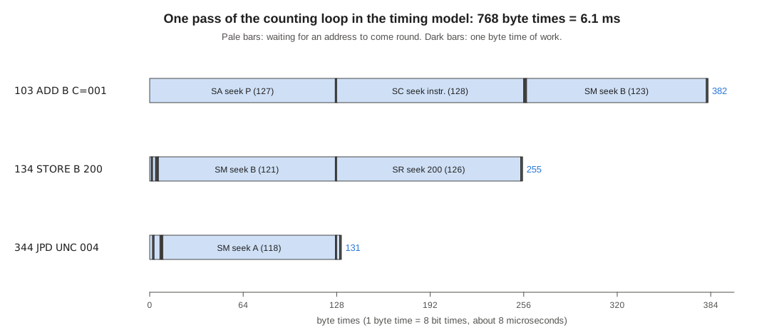
For the Programming Reference Manual’s own example — a three-instruction loop at 004–011 that adds 1 to B, stores B in the output lamps and jumps back — the model gives 768 byte times, 6.1 milliseconds, per pass: about 490 instructions a second, or about 160 counts a second in the lamps. That agrees with the manual’s remark that “the lamps will be operating too fast in the lower order positions to observe the action in detail”: the lowest lamp would flicker at about 80 Hz, while lamp 3, changing every eight counts, would be just visible as a flicker. It agrees too with the published “below 1,000”.
The model also shows where the time goes. Of the 768 byte times, the machine spends a dozen actually reading, adding and writing; the rest is spent waiting for addresses to come round. One result is striking, and should be read as a property of the model rather than a measurement: an instruction placed at 004, immediately after P at 003, is found a full revolution late, because the comparison for “next byte is 004” is made during the byte time when P is still being read. A program placed a few bytes further on would fetch faster. Whether the real machine behaves exactly so would need a working KENBAK-1 and an oscilloscope.
For scale, a contemporary minicomputer such as the DEC PDP-8 (see the Vintage Digital Computers site) executed several hundred thousand instructions a second, and the Intel 8080 of 1974 several hundred thousand. The KENBAK-1 was a thousand times slower than both. It did not need to be fast: its job was to let a person watch a program run, and at a few hundred instructions a second the lamps can be followed and a single-stepped program examined byte by byte.
3.7 Lights, Switches and Power
The rest of the machine is plain. A linear power supply produces +5 volts for the logic and the negative supply the memory clocks need; the Programming Reference Manual gives the consumption as 40 watts and notes that the machine “can be left on without damage or significant expense”. A fan cools the case, and the manual suggests listening for it to tell whether the power is on, since there is no power lamp.
The front panel carries fifteen pushbuttons, a power switch, a memory-lock toggle and twelve incandescent lamps: eight data lamps and four control lamps labelled Input, Address, Memory and Run. Blankenbaker had considered other input and output devices and rejected them on cost: “In the end, I decided I would just have, for the price, to confine myself to lights and switches.” The lamps are driven from a K register, loaded either from the W register or from memory, so that the panel can show the input byte, the address register, a memory byte or the output byte at 200 (Volume 6). The data buttons are “scanned by T0 through T7 and ORed together to produce the serial signal BU”, which is written into address 377 as it passes: even the panel’s input is serial. The switches were the weak point: “The most unreliable aspect of it was that the switches were glued to the front panel of it. Glued, I say, epoxied, and sometimes they broke loose.”
3.8 What the Design Says
The KENBAK-1 is sometimes described as primitive because it is slow. It is better described as economical, in the exact sense its designer intended. Every decision trades time, which costs nothing, for parts, which cost money. A serial adder replaces eight; a circulating memory replaces core; registers in memory replace three registers and a counter; a five-flip-flop state machine replaces a microprogram store. The result has the full shape of a stored-program computer — 256 bytes of program and data, three registers, indexed and indirect addressing, subroutine calls, conditional jumps and a console from which a program can be loaded, examined, single-stepped and run — in a box a person could carry and afford.
It was also, by a matter of months, the last of its kind. The design that replaced it put the whole control and data path on one chip, kept the registers in hardware on that chip, and used random-access memory whose price was falling every year. Within four years the Altair 8800 would offer an 8-bit processor on a chip, and a few years later random-access memory would make the shift register an oddity. The KENBAK-1 shows what a personal computer looked like when it had to be built the old way. Volume 4 tells how it was sold; Volume 6 describes the instruction set that this hardware executes; and Volume 8 describes the reproductions, some of which rebuild this board chip for chip, and one of which replaces all of it with a single microcontroller.
Next — Volume 4: Selling a Computer in 1971 — Fifty Machines and a Scientific American Advert. A corporation formed in a summer, $20,000 from five former colleagues, parts for fifty machines, an advertisement in the September 1971 Scientific American — and a market of schools whose budgets moved more slowly than a small company’s money ran out.
Comments (0)