KENBAK-1 · Volume 12
KENBAK-1 — Volume 12 — My Full-Size KENBAK-1 — The Board, the Memories and the Bill of Materials
The reproduction board gone over from its own Gerber files: where the two 1404A memories go and exactly how they fit, the 1971 schematics behind them, a line-by-line parts list with the substitutes that obsolescence and loose specifications demand, the order of assembly, the first power-up, and three programs for proving the finished machine
12.1 About This Volume
Volume 11 laid out the plan: a full-size KENBAK-1 with the original TTL logic, on Artem Kalinchuk’s reproduction board, behind a Front Panel Express panel, in a copy of Bud Radio’s Grand Prix case. Since then I have ordered the board and every part on the list, and I have decided to mill the two aluminium side rails myself rather than pay a job shop for them. I am also building Adwater & Stir’s two small emulations, the µKENBAK-1 and the nanoKENBAK-1, and each of those has its own volume after this one.
This volume is the reference for the full-size board, written before it arrives, from the files it was made from:
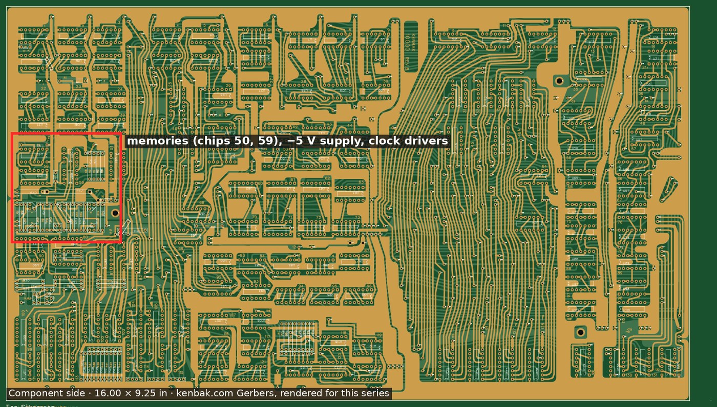
- The board, from its Gerber files: what is on it, how it compares with Kalinchuk’s, and how big it is.
- The memories, close up: the footprint of the two 1404A positions, measured from the drill file, each pad checked against Intel’s 1976 data sheet, and the two ways of socketing them.
- The schematic sections that the memories depend on (memory, clock drivers, power) and the lamp drivers, which decide what kind of LED can replace the 1971 bulbs.
- The bill of materials, line by line in the same form as the parts lists for my nixie clocks: original part, part to buy now, and why it changed.
- Assembly and bring-up, in stages, with the voltages to measure before a fifty-year-old memory chip goes anywhere near the board.
- Making the side rails, the case work I am doing in my own shop.
- Programming the finished machine: a front-panel checkout, a lamp test and a memory test for each 1404A, all run first in the series’ simulator.
Where I have done something, it is written as mine. Everything else is the reference account of how the job is done, and it will be checked against the board itself when it comes.
12.2 The Board From Its Own Files
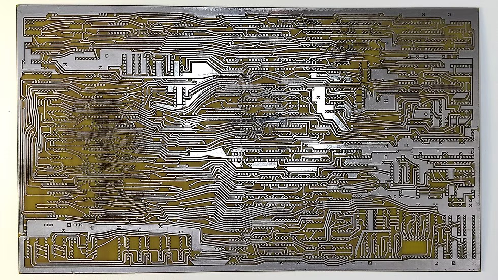
The board files for the reproduction are published free on kenbak.com, the site of the KENBAK-1 registry: copper Gerbers for the top and bottom, an Excellon drill file, and a silkscreen as both Gerber and PDF (Library copy). The author explains there that he entered Blankenbaker’s schematics in TinyCAD, exported the netlist to FreePCB, and routed the traces while looking at photographs of an original board. Kalinchuk’s listing says his board “was re-created by Thomas Jones using computer software” (Volume 8). The files themselves are stamped “FreePCB version 1.359”, and their header records the folder they were made in, C:\Users\tejon\Desktop\kenbak\CAMPCB. That user name fits a Thomas E. Jones, and the Computer History Museum catalogues a KENBAK-1 part as the gift of a Thomas E. Jones in 2022. Kalinchuk’s own repository settles the question (below).
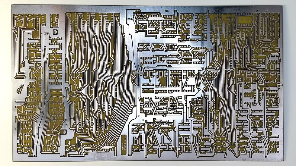
Kalinchuk publishes his own files on GitHub (github.com/kalinchuk/kenbak_1), and his README says where his board came from: “I believe it was Thomas Jones who created a reproduction PCB for the Kenbak-1. I used his copper layers to create the Gerber file.” His top-copper, bottom-copper and drill files are byte-for-byte identical to the kenbak.com files, so every render and close-up in this volume shows exactly the board I ordered. His listing photographs agree: the same legend, “KENBAK 10000 REV.B”, etched in copper; the same chip numbers etched beside each chip position; the same pattern of copper pours; and on the solder side the same long horizontal runs of traces. Like the original, his board has no solder mask and no printed component legend. The kenbak.com author recommends making it exactly that way, because the board “doesn’t need any high-precision fabrication, or any silk-screen labeling or soldering masks”. The silkscreen file exists to help a builder find parts, not to be printed.
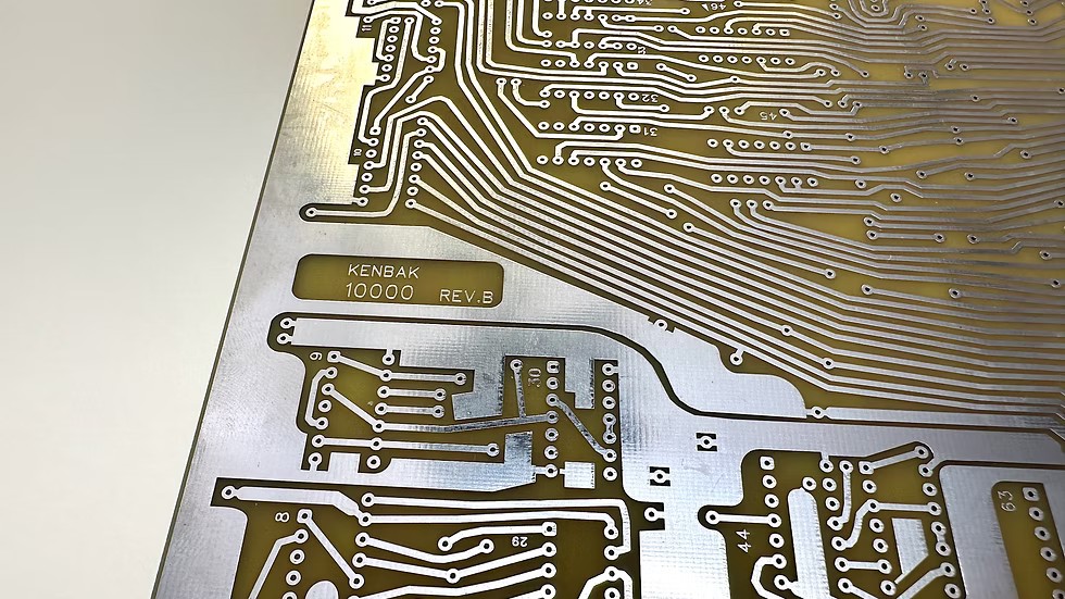
The files contain no fabrication notes, so the board’s vital statistics have to be measured from them. The figures in this volume were drawn by a small renderer written for the series (03-outputs/pcb/render_gerber.py), because none of the usual Gerber viewers was to hand. It reads FreePCB’s output directly, and its pictures match Kalinchuk’s photographs.
Table 1 — The Board From Its Own Files
| Feature | From the files |
|---|---|
| Size | 16.00 × 9.25 in (406.4 × 235.0 mm), from the outline drawn on the copper and silkscreen layers. Alignment targets half an inch outside the edge make the files look 17 in wide |
| Layers | two, with large copper pours on the component side and many on the solder side |
| Holes | 2,533, all plated: 2,525 at 0.030 in for chip pins and small parts, 5 at 0.055 in for heavier leads (the zener, the 2 W resistor and a pair near the centre), and 3 mounting holes of 0.125 in |
| Grid | every hole but one on a 0.050 in grid |
| Chip positions | 126 fourteen-pin, 4 sixteen-pin and 2 eight-pin footprints, counted from their square pin-1 pads |
| Legend | ”KENBAK 10000 REV B”, in copper |
| Jumper | one wire jumper, shown on kenbak.com’s layout picture |
The chip count settles a small disagreement between the parts lists. Stockly’s packing list has 46 type 7400 chips and kenbak.com’s has 45. The board has 130 TTL positions, which the 46 fill exactly, so 45 is one short. The three mounting holes match the three #4-40 standoffs in Stockly’s hardware list.
12.3 Where the Memories Go
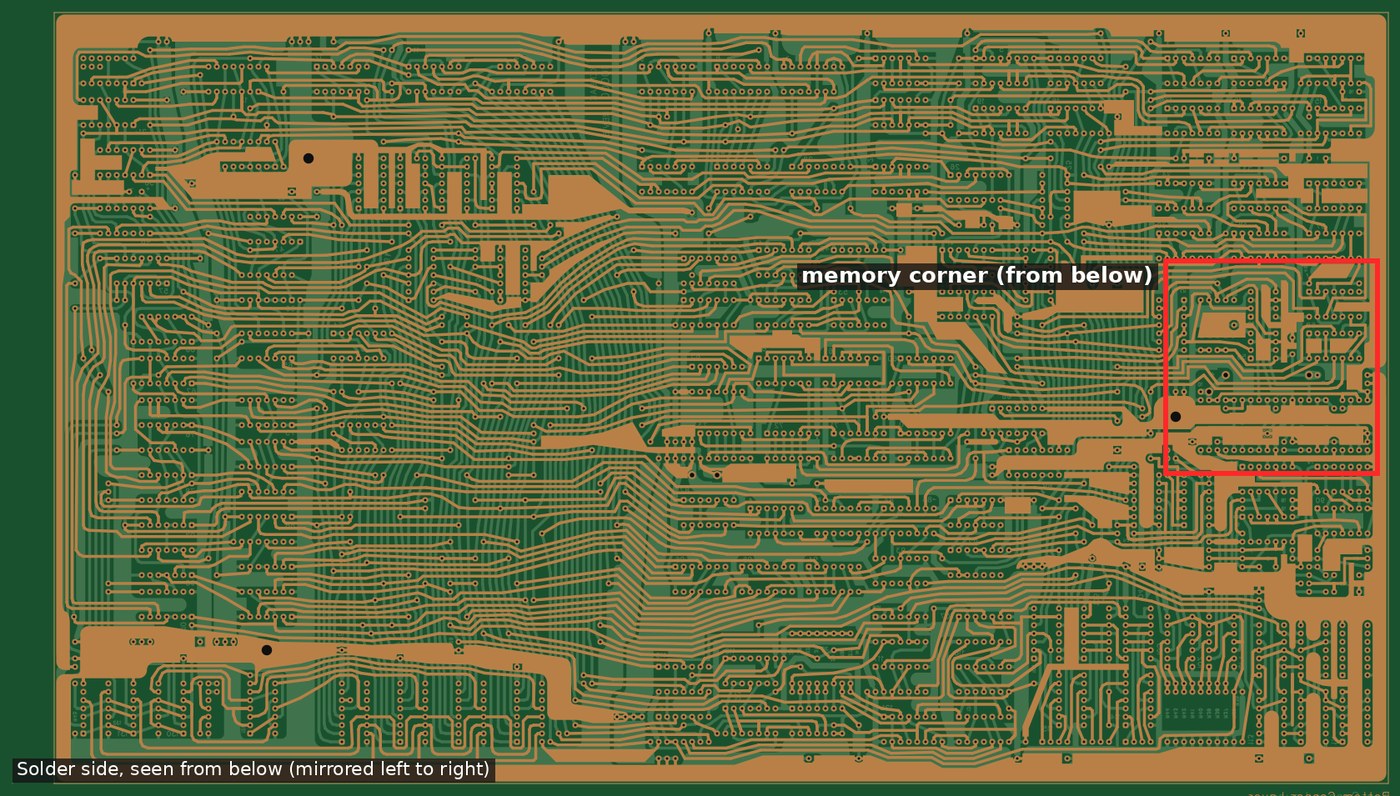
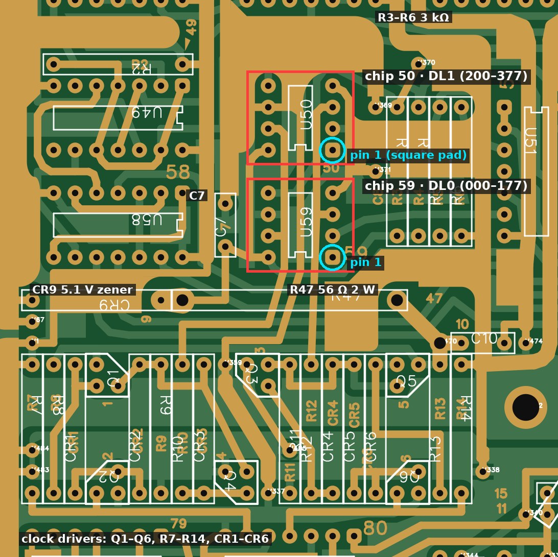
The whole of the computer’s memory, 256 bytes, is two Intel 1404A shift registers (Volume 3). On the board they sit near the left-hand edge, a third of the way up, in a corner that holds everything they need: the four 3 kΩ input pull-ups and output pull-downs, the dropping resistor and zener that make their −5 V supply, a filter capacitor, and, just below, the six transistors that turn the logic clock into the large clock swings the chips need. The positions are numbered 50 and 59 in the copper, the same numbers Stockly used for them, IC50 and IC59.
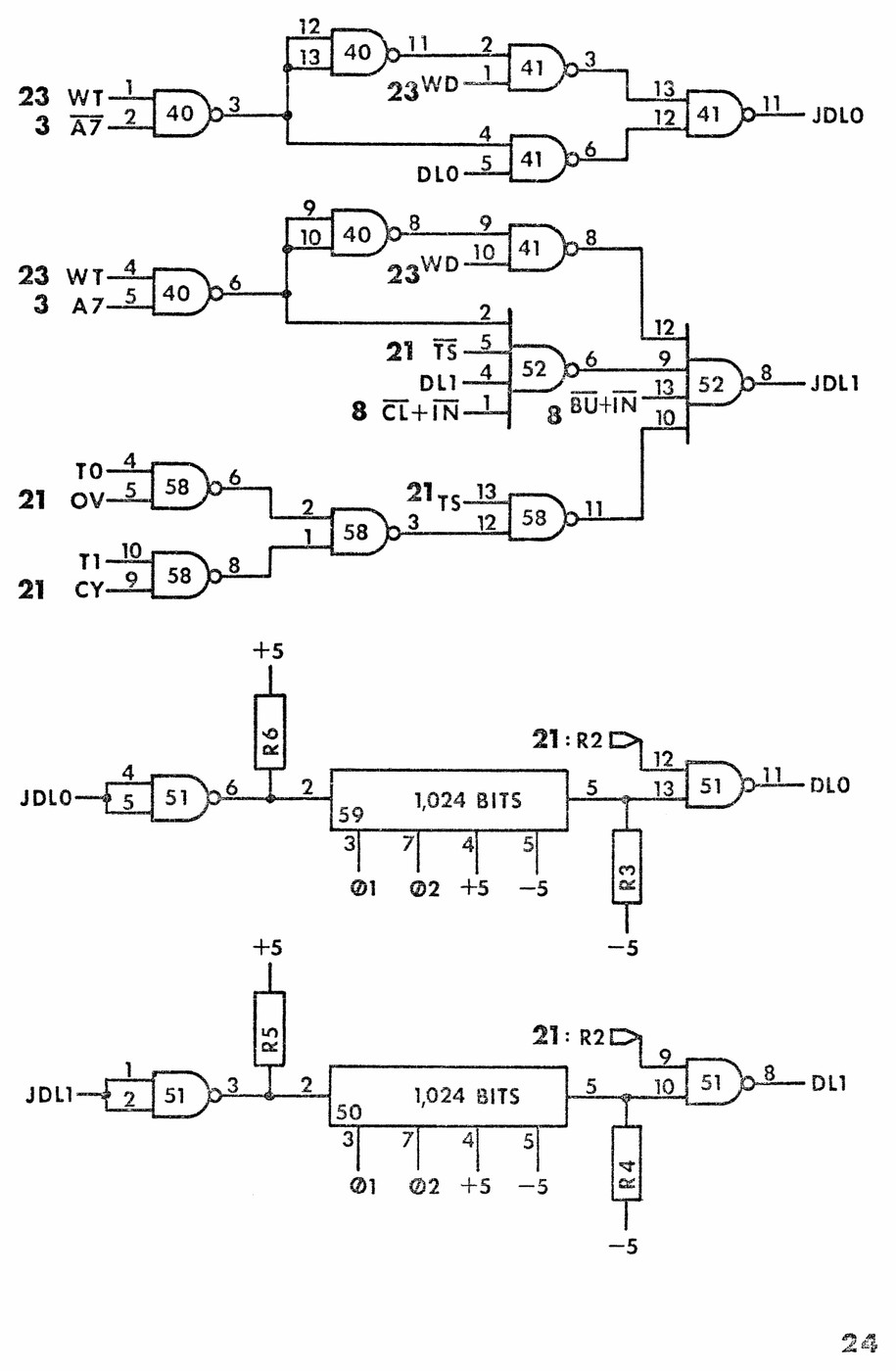
The 1971 schematic says which is which. Chip 59 is delay line 0, holding addresses 000 to 177 octal, which include the A, B, X and P registers at 000 to 003. Chip 50 is delay line 1, holding 200 to 377, which include the OUTPUT byte at 200 that drives the lamps when the machine runs. That matters when something goes wrong. A dead chip 59 stops everything, because the registers live in it. A dead chip 50 breaks the upper half of memory, which includes the OUTPUT byte the lamps show while the machine runs and the INPUT byte at 377 that the data keys write into.
12.3.1 The footprint: DIP-8, not round
Volume 11 left one question for the day the board arrives: whether the memory positions are an eight-pin DIP footprint or a round one, because that decides how the cans can be socketed. The drill file answers it. Both positions are DIP-8: two rows of four holes, the rows 0.300 in apart and the holes 0.100 in apart along each row, plated through at 0.030 in. Chip 50’s holes run from 5.6 to 5.9 in up the board and chip 59’s from 5.1 to 5.4, in two columns at 1.35 and 1.65 in from the left edge, so the two footprints sit end to end, 0.500 in (12.7 mm) apart centre to centre. There is no eight-hole circle anywhere on the board: of its 2,533 holes, every one but one lies on a 0.050 in grid, and the pins of a round TO-99 can cannot.
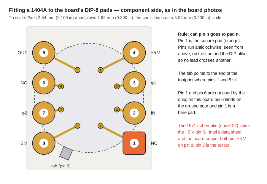
Each footprint has its pin 1 marked by the one squarish pad, at the end of the right-hand column nearer the bottom edge of the board, toward R47 and CR9. That end is where a DIP socket’s notch goes.
The board itself still has to be looked at when it arrives. Kalinchuk’s fabricator could in principle have worked from a revised file, and the photographs do not show the memory corner closely. But everything visible in them matches these files, so DIP-8 is what I expect to find.
12.3.2 Checking every pin against Intel’s data sheet
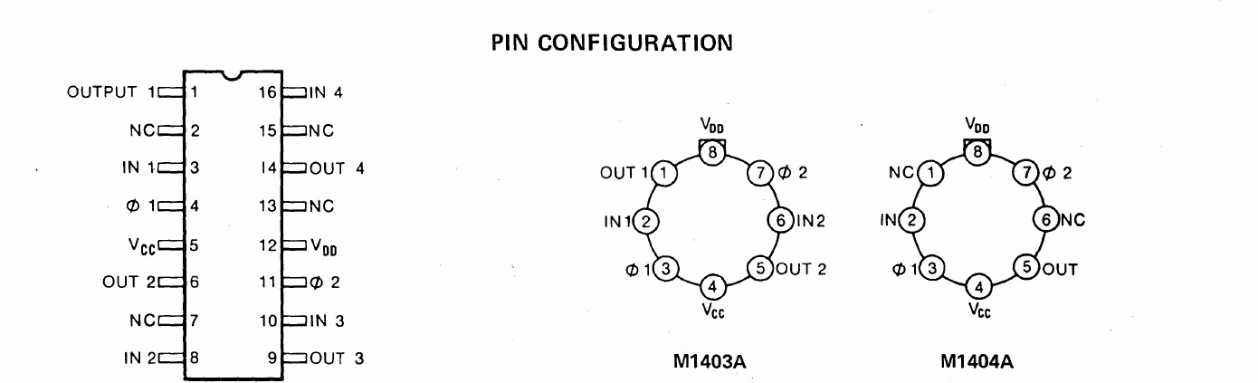
A DIP-8 footprint for an eight-lead can raises an obvious question: does pad n of the footprint carry the signal that the can’s pin n expects? The can’s leads are numbered round a circle and the DIP’s round a rectangle; get the correspondence wrong and the −5 V supply lands on an input. The series’ earlier volumes had to rely on the Synertek second-source data sheet (Library copy), because Intel’s own was not to hand. It has now been found, in Intel’s 1976 Data Catalog (preserved by bitsavers; Library copy), and it gives the metal-can pinout directly.
The board’s copper was then checked pad by pad. A second script (netcheck.py) rasterises both copper layers, joins them through every plated hole and labels each connected island of copper. That is a crude netlist, but enough to say which pads share a net and which reach the supply pours. To identify the pours, it looks at an ordinary 7400 nearby, whose pin 14 is +5 V and pin 7 is ground. With the pads numbered in the usual way for a DIP, anticlockwise from the square pad as seen from the component side:
Table 2 — The board's copper was then checked pad by pad. A second script (netcheck.py) rasterises both copper layers, joins them through every plated hole and labels each connected island of copper. That is a crude netlist, but enough to say which pads share a net and which reach the supply pours. To identify the pours, it looks at an ordinary 7400 nearby, whose pin 14 is +5 V and pin 7 is ground. With the pads numbered in the usual way for a DIP, anticlockwise from the square pad as seen from the component side
| Pad / can pin | Intel’s 1404A | What the board connects it to | Agrees? |
|---|---|---|---|
| 1 | not connected | nothing: an isolated pad on both chips | yes |
| 2 | input | a separate net for each chip | yes |
| 3 | φ1 clock | one net shared by both chips | yes |
| 4 | VCC, +5 V | the pour that also feeds 7400 pin 14 | yes |
| 5 | output | a separate net for each chip | yes |
| 6 | not connected | the ground pour (7400 pin 7) | harmless |
| 7 | φ2 clock | one net shared by both chips | yes |
| 8 | VDD, −5 V | one shared net that also reaches C7, CR9 and the pull-down resistors R3 and R4 | yes |
The answer is clean: the board’s DIP-8 pad n is wired for the can’s pin n, with both drawings read as top views. That also settles the other open question from the socket notes, whether Stockly’s pin drawing was a top or a bottom view. Intel draws the can from above with its pins running anticlockwise. A DIP’s pins run anticlockwise from above too, so the leads of a can bent outward drop into the DIP holes in order, without crossing.
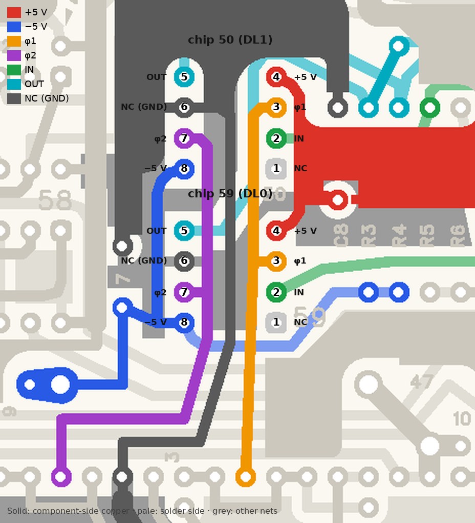
Two traps are worth recording. First, the 1971 schematic itself is wrong about one pin. Sheet 24 shows the −5 V connection of both chips at pin “5”, the same number as the output. The board, like Intel’s sheet, puts −5 V on pin 8, and anyone wiring from the schematic alone would put −5 V on an output. Second, the Synertek data sheet’s eight-pin drawing is not the can. It shows Synertek’s plastic DIP version, the SYP1404A, which numbers its pins differently (1 output, 2 φ2, 4 VDD, 5 input, 6 φ1, 8 VCC). It is a good data sheet for the electrical figures, but the wrong drawing for this job.
12.3.3 Fitting the cans: the two methods on this board
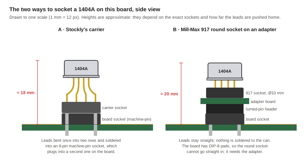
With a DIP-8 footprint, the two socketing methods from Volume 11 change places. Stockly’s carrier plugs straight in. The round Mill-Max socket cannot go straight in, and needs its small adapter board. My board confirms what the files show: both memory positions are DIP-8, and the square pad is pin 1. I am fitting my memories by Method A: each can soldered into a machined DIP socket, which plugs into a second machined socket soldered to the board.
Method A, the carrier. Bend each lead of the can once, outward, into two rows that match an eight-pin machine-pin DIP socket, and solder the can into that socket, which becomes a plug. A second machine-pin socket goes on the board, with its notch at the square-pad end. The orientation rule is short: with the can upright, its tab points toward the notch, between pins 8 and 1. Before the carrier goes anywhere near the board, check with a meter that each turned pin on its underside connects to the can lead of the same number, with nothing shorted to the case. Stockly’s warning about heat holds: solder briefly, or the plastic softens and the pins move.
Method B, the round socket on an adapter. Mill-Max’s series 917 socket (917-43-108-41-005000 through-hole, -001000 surface-mount) takes the can with its leads straight. On this board it needs a small adapter: the 917 on top, two rows of four turned header pins underneath that plug into the board’s DIP socket, and round pad n wired to DIP pin n. The two footprints are only 12.7 mm apart along the column, so each adapter must be under 12.7 mm (0.500 in) in that direction, about 0.48 in to leave a gap. The 0.600 × 0.550 in sketch in my socket notes must be laid out with its 0.600 in side across the columns, and the 0.550 in side trimmed to fit, or the two adapters will collide. The 917’s round body is 10 mm across, so 0.48 in leaves room.
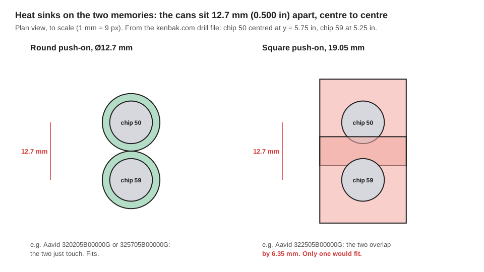
Heat sinks. Stockly fitted a push-on finned sink to each can. The 1971 machine had none, but these parts are fifty years old and cannot be replaced, so a sink is cheap insurance. The two cans are only 12.7 mm apart, which rules out a 19.05 mm square TO-5 sink (Aavid 322505B00000G): two of them would overlap by 6.35 mm. Round push-on sinks 12.7 mm across, such as Aavid’s 320205B00000G or 325705B00000G, just touch, and they are the size to buy. Check the can’s diameter against the sink’s bore first. The 1404A is a TO-99 style can, 8.5 to 9.4 mm across under the flange.
Before fitting either, measure a lead. The through-hole 917 grips leads of 0.018 to 0.025 in; the surface-mount version, 0.015 to 0.025 in. TO-99 leads are nominally 0.016 to 0.021 in, so a thin one may need the surface-mount socket. Machine-pin DIP sockets grip a wide range. The board’s 0.030 in holes take ordinary socket tails with room to spare.
12.4 The Schematic Behind the Memories
The 1971 Theory of Operation manual (Library copy) gives the complete logic in 26 sheets. Volume 3 explains how the machine works as a serial computer and reproduces its block diagram. This section covers only the four sheets a builder reads with a meter in hand.
12.4.1 Sheet 24: the memory
Each memory’s input is driven by a gate of chip 51, with a 3 kΩ pull-up to +5 V (R5, R6) that lifts the TTL high level towards the 3.5 V or more that the MOS input needs (Intel: at least VCC − 1.5 V). Each output has a 3 kΩ pull-down to −5 V (R3, R4), which is Intel’s standard test load for driving TTL, and goes on through another gate of chip 51. The gating above them decides, bit by bit, whether a byte is recirculated or replaced. All four 3 kΩ resistors are in the memory corner, beside the chips.
12.4.2 Sheet 25: the clock and the clock drivers
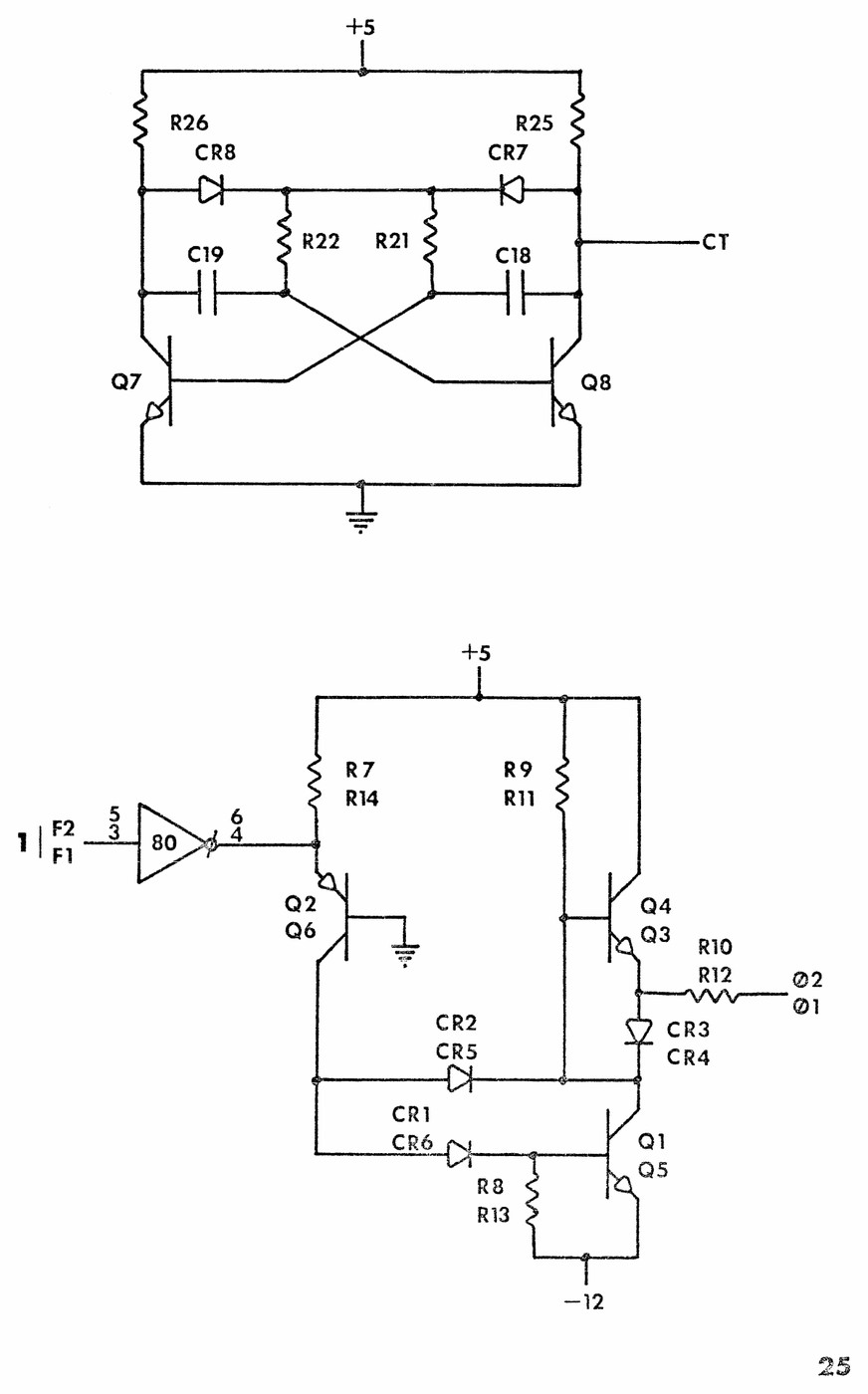
A two-transistor multivibrator, Q7 and Q8, runs at about 2 MHz. It is divided down to the 1 MHz bit rate, and kenbak.com warns that its timing capacitors may need changing to get there. Two identical driver chains, one per clock phase, turn TTL-level phases F1 and F2 into the swings the 1404As need. Each chain is a 7416 gate (chip 80), a PNP common-base stage (Q2 or Q6), an NPN emitter follower to +5 V (Q4 or Q3) and an NPN pull-down to −12 V (Q1 or Q5), with series resistors to the clock pins. Intel’s sheet asks for a clock-low level of 15 to 17 V below VCC, that is about −10 to −12 V, which is why the machine needs a −12 V supply at all.
12.4.3 Sheet 26: power
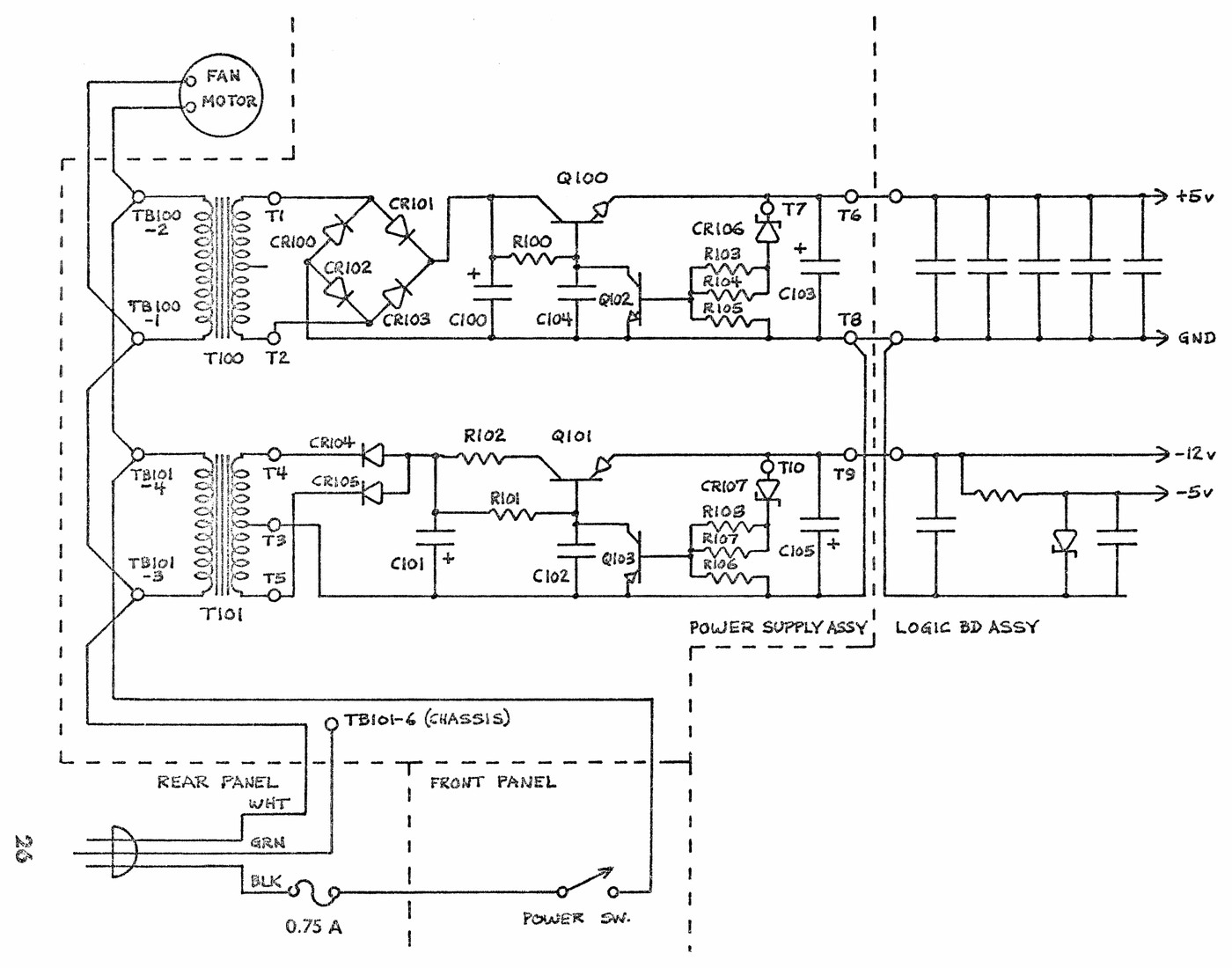
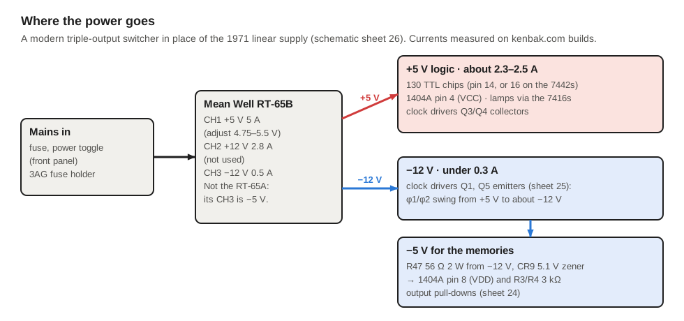
The original supply was linear, with two transformers, two pass transistors and a fan, and drew about 156 W from the wall to deliver perhaps 15 W, according to kenbak.com’s measurement. Only two rails come onto the logic board: +5 V, about 2.3 to 2.5 A on a working board, and −12 V, under 0.3 A. The memories’ −5 V is made on the board, from −12 V, by R47 (56 Ω) and the 5.1 V zener CR9, with C7 across it. Those are the two heavy parts in 0.055 in holes just below the memories. Both current kits use a switching supply instead, and so will I.
12.4.4 Sheet 07: the lamps
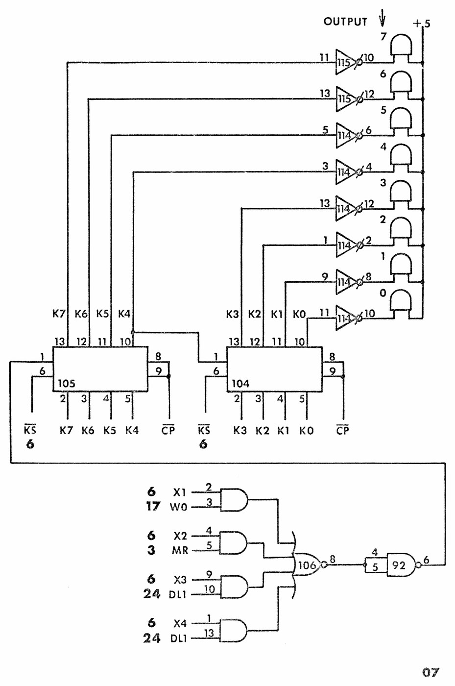
The eight data lamps are wired straight from +5 V to open-collector 7416 outputs (chips 114 and 115), with no resistor. That one fact decides the lamp question in the parts list. An incandescent bulb is its own current limiter, but an LED is not, so a plain LED in a bulb’s place would draw whatever the 7416 can sink and burn out. The original Type 680 bulb is rated at 60 mA, more than the 7416’s 40 mA data-sheet rating, which is presumably why kenbak.com asks for lamps under 40 mA.
12.5 The Bill of Materials
The kit is sold out, so I bought the board alone and every other part line by line. This list starts from Stockly’s 2007 packing list (Library copy) and parts-placement guide (Library copy; the most complete count of a KENBAK-1), checks it against the board and the 1971 schematics, and adds kenbak.com’s list where the two differ. For each line it gives the original part, the part to buy now, and why it changed. A printable version with tick boxes is at the end of this volume (Printable Bill of Materials), with an assembly drawing of the board that shows where every designator goes. Stock and prices change daily, so none are given; part numbers are examples that meet the specification. Availability was read on 2 November 2026.
Table 3 — The Bill of Materials
| Tag | Meaning |
|---|---|
| Same | The original part, or a direct equivalent, is still a standard item |
| EOL | The original is obsolete: buy new old stock or a replacement |
| Spec | The original list does not say enough, or the rating is wrong for a modern build |
| Conflict | The lists, the schematic or the board disagree; the resolution is given |
| Choice | A change made for this build |
12.5.1 Memory
Table 4 — Memory
| Qty | Where | Original | Buy now | Tag | Why |
|---|---|---|---|---|---|
| 2 (+2 spares) | Chips 50 and 59 | Intel 1404A, 1,024-bit dynamic shift register, 8-lead metal can | 1404A, metal can, second-hand (eBay); AMD and Synertek second-source parts carry the same number | EOL | Out of production for decades. Not the 1401A, which kenbak.com’s own list once gave in error.1 I bought four, two to fit and two spares. Check the can’s markings for “1404A”, and test each part in the machine with the memory test below before relying on it |
| 4–6 | Board sockets, and carriers if using Method A | none (soldered in 1971) | 8-pin machine-pin DIP sockets, 0.300 in | Choice | Two on the board and two as carriers; buy six. They also take the Method B adapter |
| 2 | Method B, trial | none | Mill-Max 917-43-108-41-005000 (through-hole) or -001000 (surface-mount, for the adapter) | Choice | Round 8-contact socket on a 0.200 in circle. Needs an adapter on this board’s DIP-8 footprint, under 12.7 mm along the column. Not 917-…-208, which is the larger TO-100 circle |
| 2 (4) | On the cans | none | Round push-on TO-5 heat sink, Ø12.7 mm: Aavid 320205B00000G or 325705B00000G | Conflict | My list had a 19.05 mm square sink (Aavid 322505B00000G), but the cans are 12.7 mm apart and two of those would overlap (figure above). Round 12.7 mm sinks just touch |
12.5.2 TTL logic
Buy standard 74-series parts: 7400, not 74LS00 and never 74HC00. The kenbak.com builders were told the faster families “may not work” and never tried them in this design.1 74HC is CMOS, with different thresholds and different behaviour from unconnected inputs, and two of the types used here have no HC equivalent at all. Of the fourteen types, Texas Instruments still lists only the 7400, 7404 and 7416 as active products. The other eleven no longer have TI product pages, so they are new-old-stock buys from dealers such as Jameco, Unicorn Electronics or eBay.2 Plan to test every chip, or at least to have spares of the types used most.
Table 5 — TTL logic
| Qty | Where | Original | Buy now | Tag | Why |
|---|---|---|---|---|---|
| 46 | Throughout | 7400 quad 2-input NAND | SN7400N (TI, active) | Conflict | kenbak.com lists 45; the board has 130 TTL positions and Stockly’s 46 fill them exactly |
| 15 | 7410 triple 3-input NAND | 7410, new old stock | EOL | ||
| 13 | Registers (I, W, K, L and more) | 7495 4-bit shift register | 7495 or 7495A, new old stock | EOL | The A suffix is the later version of the same part. 74LS95B is a different family; untested |
| 10 | 7474 dual D flip-flop | 7474, new old stock | EOL | ||
| 10 | State logic | 7454 4-wide AND-OR-INVERT | 7454, new old stock only | EOL | The 74LS54 is not a substitute: its gate arrangement differs from the 7454’s. This is the type to hunt for first |
| 10 | 7430 8-input NAND | 7430, new old stock | EOL | ||
| 9 | 7420 dual 4-input NAND | 7420, new old stock | EOL | ||
| 4 | Decoders | 7442 BCD-to-decimal, 16-pin | 7442 or 7442A, new old stock | EOL | The only 16-pin chips: power on pins 16 and 8 |
| 3 | Inverters | 7404 hex inverter | SN7404N (TI, active) | Same | |
| 3 | Chips 80, 114, 115: clock and lamp drivers | 7416 hex inverter, open collector, 15 V | SN7416N (TI, active) | Same | No HC equivalent. It sinks the lamps and drives the clock-driver transistors |
| 3 | 7486 quad XOR | 7486, new old stock | EOL | ||
| 2 | Chips 102, 103 | 7403 quad NAND, open collector | 7403, new old stock | EOL | A 74HC03 is open-drain CMOS and not a drop-in for open-collector wired logic |
| 1 | 7408 quad AND | 7408, new old stock | EOL | ||
| 1 | 7451 dual AND-OR-INVERT | 7451, new old stock | EOL | Obsolete at TI; buy a spare |
12.5.3 Transistors and diodes
Table 6 — Transistors and diodes
| Qty | Where | Original | Buy now | Tag | Why |
|---|---|---|---|---|---|
| 6 | Q1, Q3, Q4, Q5 clock drivers; Q7, Q8 multivibrator | TI 2N5449 NPN (Stockly: 2N4401) | 2N4401 (onsemi and others) | EOL (original) | The TI part is long gone; Stockly’s 2N4401 (40 V, TO-92) has run in kits since 2007.1 Q1/Q5 swing to −12 V, so the collector sees about 17 V, well within its rating. Lead order varies between TO-92 types, so check against the board outline before fitting |
| 2 | Q2, Q6 common-base clock stages | TI 2N5447 PNP (Stockly: MPS3702) | MPS3702 if found; otherwise 2N3906 | EOL | The 2N3906 (40 V, faster) is the usual substitute. Both are commonly wired E-B-C in TO-92, but makers differ, so check the data sheet of the part actually bought against the board outline |
| 8 | CR1–CR8 | 1N914 | 1N4148 | Same | The same diode under a later number |
| 1 | CR9, −5 V zener | ”5.1 V zener, 0.75 W min” (kenbak.com: “Grant used an IN7433”) | 1N4733A (5.1 V, 1 W, DO-41) | Spec | ”IN7433” is a typo for 1N4733. R47 passes about (12 − 5.1)/56 = 123 mA; with the memories unplugged the zener takes all of it, about 0.63 W, so a 1 W part is right and a 0.5 W one is not. It fits the board’s 0.055 in holes |
12.5.4 Resistors
Carbon film or metal film, 1/4 W unless noted. The values are Stockly’s, with designators from his placement guide; the board’s silkscreen uses the same R numbers.
Table 7 — Resistors
| Qty | Where | Original | Buy now | Tag | Why |
|---|---|---|---|---|---|
| 27 | R1, R2, R9, R11, R15, R17, R20, R27–R46 | 1 kΩ | 1 kΩ | Same | R27–R46 stand in two blocks near the bottom edge of the board |
| 4 | R3–R6, memory | 3 kΩ | 3 kΩ | Same | Intel’s TTL load is 3 kΩ to VDD |
| 4 | R7, R14, R21, R22 | 270 Ω | 270 Ω | Same | Clock drivers and multivibrator |
| 2 | R8, R13 | 220 Ω, 1/2 W | 220 Ω, 1/2 W | Same | Pull-downs to −12 V in the clock drivers |
| 4 | R10, R12, R18, R19 | 120 Ω | 120 Ω | Same | R10 and R12 are the series resistors to the φ2 and φ1 pins |
| 2 | R25, R26 | 68 Ω | 68 Ω | Same | Multivibrator collector loads |
| 1 | R47, −5 V dropper | 56 Ω, 2 W | 56 Ω, 2 W metal oxide or wirewound | Spec | It dissipates about (12 − 5.1)²/56 = 0.85 W, rising to about 1 W if the −12 V rail sits 5 % high. 2 W is the minimum; mount it a few millimetres off the board. Leads go in 0.055 in holes |
| — | R15 | 1 kΩ (Stockly) | 1 kΩ, with a 3 kΩ on hand | Conflict | kenbak.com used 3 kΩ, a value “arrived at by experiment”; Stockly’s kits used 1 kΩ. Fit 1 kΩ first. If the machine misbehaves where this part matters, try 3 kΩ. A pair of socket pins in R15’s holes makes the swap easy |
12.5.5 Capacitors
The packing list’s capacitor voltages are a mix of whatever was to hand (a 100 µF at 100 V on a 5 V rail, for example) and need sense rather than copying. The rules are simple: an electrolytic on a +5 V node needs 10 V or more, one on the −12 V node 25 V or more, and one on the −5 V node 10 V or more, 16 V for margin. On the negative rails the electrolytic’s positive lead goes to ground. The marking on a negative rail’s capacitor is the easiest one to get backwards. Higher voltage ratings are harmless if the can fits its holes and its space.
Table 8 — Capacitors
| Qty | Where | Original | Buy now | Tag | Why |
|---|---|---|---|---|---|
| 25 | C2, C3, C5–C8, C11–C13, C20–C22 and bypass | 0.1 µF | 0.1 µF 50 V X7R, 0.2 in lead spacing | Same | Ceramic bypass across the supply |
| 2 | C18, C19, multivibrator | 1,500 pF (“0.0015 µF disc”; 1,000 pF also listed) | 1,500 pF C0G/NP0, plus 1,000 and 2,200 pF to tune | Spec | These set the multivibrator’s 2 MHz, which is divided to the 1 MHz bit rate. kenbak.com notes that they may need changing to get there; C0G holds its value with temperature |
| 2 | C16, C17, underside | mica, “about 10–6,800 pF” (one original 10 pF; Stockly 6,800 pF) | 6,800 pF silver mica or C0G, 0.2 in spacing | Conflict | Fitted on the solder side in 1971. kenbak.com reports that its machines run without them. Fit Stockly’s value |
| 4 | C1, C10, C14, C15 | 100 µF 100 V (Stockly) | 100 µF 25 V, 105 °C | Spec | 25 V covers any of these positions; 100 V is needlessly large |
| 2 | C4, C9 | 100 µF 25 V | 100 µF 25 V | Same | |
| 3, 1, 1 | Alternates per placement guide | 33 µF 50 V; 100 µF 50 V; 220 µF 100 V | as listed, or the same values at 25 V | Spec | The placement guide allows alternates in C1, C4, C9, C14 and C15. kenbak.com’s list calls for a 33 µF 6.3 V; anywhere near the −5 V or −12 V lines that is too little, so buy 16 V or more |
| 2 | Store and Read Memory switches | electrolytic ”??? µF”, on the back of the front panel | leave off at first | Spec | The value was never recorded; kenbak.com reports that its machines work without them. If the switches double-act, fit small debounce capacitors then |
12.5.6 Sockets and connections
Table 9 — Sockets and connections
| Qty | Where | Original | Buy now | Tag | Why |
|---|---|---|---|---|---|
| 126 | 14-pin positions | none (soldered in 1971) | 14-pin machined (turned-pin) DIP sockets, 0.300 in | Choice | So that new-old-stock chips can be swapped while debugging. I use only machined sockets, on this board and every build: they are more robust than stamped dual-wipe sockets, make better contact, hold the chips more firmly, and look better |
| 4 | Chips 125–128 (7442) | none | 16-pin machined (turned-pin) DIP sockets | Choice | Machined, like the rest |
| 1 strip | Front-panel connections | point-to-point wires (1971) | 0.1 in single-row header, about 32 pins | Choice | So the panel unplugs from the board, as on Stockly’s kit and the kenbak.com builds: two 8-pin switch groups, a 14-pin lamp group and two single pins |
| 5 + 50 | Mating connectors | none | Molex KK 254 housings (22-01-3087 8-pos, 22-01-3147 14-pos) and 08-50-0114 crimp contacts | Choice | Polarised, so the two 8-pin switch connectors cannot be swapped by mistake without noticing |
| 1 | The board’s one jumper | wire | insulated wire link | Same | Its position is shown on kenbak.com’s layout picture |
12.5.7 Front panel and controls
My panel is Artem Kalinchuk’s Front Panel Express design, from the Case folder of his GitHub repository, so his finished machine shows what mine should look like from the front.
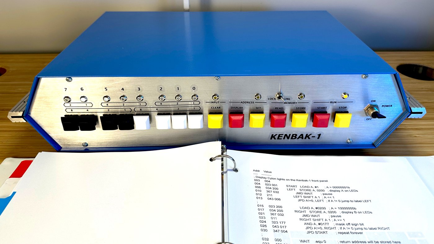
Table 10 — Front panel and controls
| Qty | Where | Original | Buy now | Tag | Why |
|---|---|---|---|---|---|
| 1 | Front panel | painted Bud panel, screen printed | Front Panel Express, engraved, from Artem Kalinchuk’s design file (the Case folder of github.com/kalinchuk/kenbak_1) | Choice | Ordered. The cutouts below are measured from that file’s preview drawing |
| 1 | Rear panel | Bud panel, perforated for the fan | Front Panel Express, from Kalinchuk’s design file | Choice | Ordered. The 1971 fan is not needed with a switching supply, but see “Heat” below |
| 15 | Keys | Raytheon reed keyswitches (KBSR series, 1969) with square caps | Cherry MX-style plate-mount keyswitches with square caps | Spec | The panel’s fifteen key cutouts are 13.97 mm (0.550 in) square, the standard 14 mm plate cutout for Cherry MX-style switches, and Kalinchuk’s kit and finished machine use MX-style switches with tall square caps (his: four black and four white data keys, red and yellow function keys). MX switches clip into a plate about 1.5 mm thick. Bud’s drawings call for 20-gauge steel panels (0.91 mm) and the shared 3D panel is 1.2 mm, but a Front Panel Express panel is ordered by thickness, and mine is 2 mm. That is about 0.5 mm too thick for the switches’ clips to catch behind it. The first test is to push one switch into the panel and see whether it holds. If it does not, mill a pocket 0.5 mm deep on the back of the panel around each cutout, about 16 mm square, a little larger than the 14 mm hole so the clips have a ledge to catch, leaving 1.5 mm at the cutout; the keys sit about 19 mm apart, so there is room. A dab of epoxy or hot-melt glue behind each switch is the fallback. The Adwater & Stir full-size replica also used Cherry MX |
| 12 | 8 data + 4 control lamps | Type 680 bulb, T-1 wire terminal, 5 V 60 mA, in a front-relampable holder with screw-on lens (white lenses for data, yellow for control) | 3 mm (T-1) LEDs with a built-in 5 V resistor, e.g. Kingbright WP710A10YD5V (yellow, about 13 mA), in chrome-bezel holders for a 3 mm LED: I am using Tayda A-6044 (chrome-plated brass with a nut, specified for a 6 ±0.2 mm hole). The panel’s twelve lamp holes are 5.9 mm across, and a nut-clamped holder doesn’t mind 0.1–0.2 mm of slop. Alternatives: Tayda A-661 (MPN LH3, 5.7 mm hole; its plastic insert A-7116 is sold separately) or Switch Electronics’ 3 mm metal prominent bezel (5.8 mm hole). Kalinchuk’s kit shipped twelve chrome-bezel indicators with grey bodies, part number not published, and none of the big holder makers (Keystone, Lumex, VCC, Bivar) offers a chrome 3 mm holder; theirs are black nylon snap-ins | Choice | The drivers have no series resistor (sheet 07), so an LED must carry its own. A 680 at 60 mA also exceeds the 7416’s 40 mA rating. Anode to the +5 V common. If original-style holders are used, bend the LED’s leads to the holder’s contacts as the 1971 manual describes for bulbs |
| 1 | LOCK toggle | miniature toggle | miniature SPST toggle with a ¼ in bushing (the panel’s hole is about 6.3 mm), plus a white boot | Same | In series with the Store key, as a write-protect |
| 1 | Power toggle | large toggle, mains | mains-rated toggle (125/250 VAC, 3 A or more) with a 15/32 in bushing (the panel’s hole is 11.75 mm) | Spec | It switches the supply’s mains input |
12.5.8 Power and hardware
Table 11 — Power and hardware
| Qty | Where | Original | Buy now | Tag | Why |
|---|---|---|---|---|---|
| 1 | Supply | linear: two transformers, Q100/Q101, fan, about 156 W from the wall | Mean Well RT-65B: +5 V 5 A, +12 V 2.8 A, −12 V 0.5 A, 129 × 98 × 38 mm3 | Choice | Board draws about 2.3–2.5 A at +5 V and under 0.3 A at −12 V.1 Not the RT-65A, whose third output is −5 V: the clock drivers need −12 V. Mean Well recommends at least 10 % load on the 5 V output when several outputs are used, which the board easily provides. Trim +5 V to 5.0–5.1 V at the board, not at the supply. Kalinchuk’s kit used an Integrated Power Designs supply instead (Digi-Key 1010417CHCO, named in his README); its ratings were not checked for this volume |
| 1 + 2 | Fuse | 3AG ¾ A (Littelfuse 3AG, Bussmann AGC) | 3AG slow-blow, 1.5–2 A (e.g. Littelfuse 313 series) | Spec | The ¾ A fast fuse suited a linear supply. A switcher’s cold-start inrush (Mean Well: 50 A at 230 VAC) can blow a fast fuse; the supply has its own internal fuse |
| 1 | Mains lead | 3-wire cord, grommet | 3-wire cord with a strain relief; earth to the chassis | Same | |
| 3 | Board mounting | standoffs | #4-40 × ½ in standoffs, screws, nylon washers | Same | The board has three 0.125 in mounting holes |
| 2 | Side rails | Bud 148 extrusions | machined from 6061 bar (next section) | Choice |
Heat. The original’s fan cooled a linear supply that wasted well over 100 W. A switching supply wastes perhaps 5 W, but the board itself still turns about 12 W into heat in a closed steel box. Stockly measured one 7400, chip 99, at about 190 °F (88 °C), and three others at about 136 °F, and supplied clip-on DIP heat sinks for the hottest few. Measure after an hour with the lid on before deciding whether to fit them, or a quiet fan in the original position.
12.6 Building the Board, in Stages
The kenbak.com authors built five of these boards and say that none worked when first switched on. Cold joints were the commonest fault. The order below is meant to find faults while they are still easy to find.
- Inspect the bare board. Hold it to a light and look for etching faults: bridges between the close traces in the long runs, and breaks. With a meter, check that +5 V (any 7400’s pin 14) and ground (pin 7) are not shorted, and that neither is shorted to −12 V or −5 V (the memory pads 8).
- Low parts first: the jumper, the resistors, the 1N4148s and CR9, C16 and C17 on the underside, then the ceramic capacitors. Leave R15 socketed.
- Sockets. All 130 TTL sockets and the two board sockets for the memories, notches toward the square pads. Solder two corner pins, check that the socket is flat, then do the rest. Over 1,800 joints go in here, so take breaks; this is where cold joints come from.
- Transistors, electrolytics, R47. Check each transistor’s lead order against the outline before soldering, and each electrolytic’s polarity twice on the negative rails.
- Headers for the front panel.
- Power, with no chips fitted. Connect the supply. Check +5 V and −12 V at the board, then −5 V at pad 8 of both memory sockets, measured to pad 6 (ground). Expect about −5.1 V, and about −12 V at the far end of R47. Check that +5 V appears at pad 4 and at pin 14 of every 14-pin socket (pin 16 of the 7442s). Pad 2 should read close to +5 V through its pull-up, pad 5 close to −5 V through its pull-down, and pad 1 nothing.
- TTL chips, all except the memories. Power up and check the clock: the multivibrator at about 2 MHz, the bit-time ring counter stepping at 1 MHz. Trim C18 and C19 if needed. Then check the memory clock pins, pads 3 and 7: square waves swinging from about +5 V down to about −12 V. The 1404As are MOS parts, and these levels must be right before the chips go in.
- Front panel. Wire it and plug it in. With no memories fitted the machine can do almost nothing, because its registers and its input byte live in memory, so the panel checkout waits for the next step.
- Power off, fit the two 1404As in their carriers or adapters, tabs toward the notches, heat sinks on. Power up and run the checkout and the programs in the last section.
Debugging. A KENBAK-1 is a serial machine, so a meter shows only averages. kenbak.com’s advice is that the only reliable way to debug one is “with a logic analyzer and lots of patience”. Failing that, a two-channel oscilloscope triggered on the bit-time T0 will show bytes going by. The memory test below narrows a fault to one memory chip. Swapping the two 1404As then shows whether a fault follows the chip or stays with the board.
12.7 Making the Side Rails
I am making the two side rails myself instead of buying them from PCBWay. Volume 11 gave the rail’s outline from Bud Radio’s drawings (Library copies: case set, rail set) and the two machines in my shop that could cut it. This section is the shop plan: what the drawings and the shared 3D model actually specify (they disagree in two places), what bar to buy, the order of operations on each machine, the cutters with speeds and feeds, how the rail fastens to the case, and how to finish it.
I am cutting them on my HiTorque 3990 mini mill, and I am buying a slitting saw for the slot and the grooves. The plan below gives the router’s version too, for anyone without a mill.
12.7.1 What the drawings and the model actually say
There are three sources for the rail. Bud’s drawings 148 (the extrusion assembly, 1975), 148-A (the cut extrusion, 1975) and 148-B (the cross-section, 1978) came to Chris Davis from Bud Industries; he added metric dimensions and notes and shared them with a 3D model of the rail, SidePiece, on PCBWay’s community site (KENBAK-1 Case). The model was measured in FreeCAD for this volume and checked against the drawings and against the model of the case halves, CaseTopBottom, which the rail has to fit.
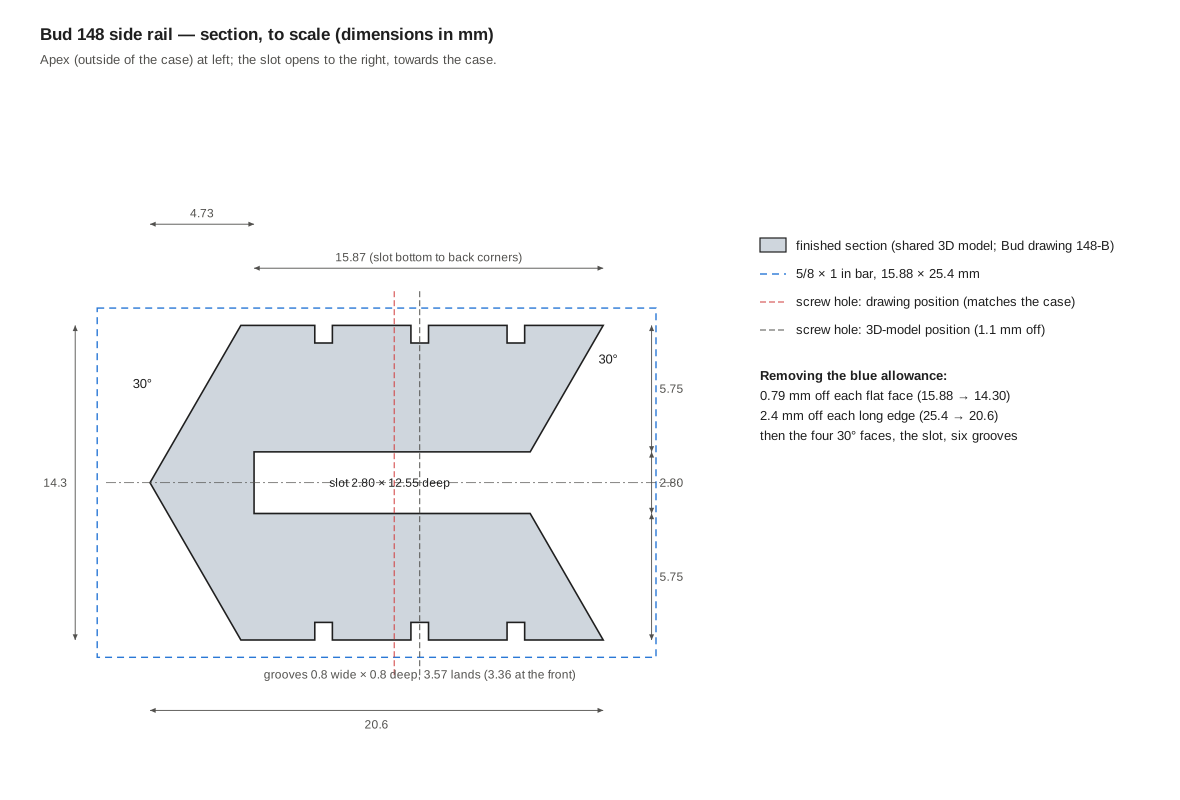
The section is not a plain bar with a slot. The outer face comes to a point made by two faces at 30° to the vertical, and the inner face, the one towards the case, has a matching notch: two faces at the same 30° meeting at the slot’s mouth. The case halves are bent at 60° along each side, so their sloping edges lie in that notch and their flat flanges go into the slot.
Table 12 — What the drawings and the model actually say
| Feature | Drawing 148-B / 148-A | 3D model | Use |
|---|---|---|---|
| Section | 20.6 × 14.3 mm | 20.60 × 14.30 | 20.6 × 14.3 |
| Slot | 2.79 high, walls 5.74 | 2.80, walls 5.75 | 2.80 |
| Slot bottom to back corners | 15.87 | 15.87 | 15.87 |
| Slot depth from its mouth | (not given) | 12.55 | 12.55 |
| Faces | 30° from vertical | 30.0° | 30° |
| Width of each flat face | 16.66 | 16.47 | 16.47 (see below) |
| Grooves | 0.8 wide, 0.8 deep, 3.57 lands | same; first land 3.36 | as the model |
| Holes | Ø3.2 through, 23.85 from each end, 9.5 mm from the edge | Ø3.2 through, 23.85 from each end, 8.34 from the back edge, Ø5.5 × 2.0 counterbore both faces | 9.5 from the back edge |
| Ends | ”Close ends via CNC milling — do not use plugs” | slot runs out through both ends | see “Closing the ends” |
Two of these need a decision.
The flat faces. The drawing’s 16.66 mm would put the front corners 3.94 mm behind the point; the 30° faces put them 4.13 mm behind it, which is what the model does. The 30° angle is the dimension that matters, because the case’s 60° bends must lie flat in the notch, so the model’s 16.47 mm is the one to cut. The difference only moves the first groove’s land from 3.57 to 3.36 mm.
The screw hole. The case model has a 3.2 mm hole in each flange, 6.40 mm from the flange’s edge and 219.0 mm apart, exactly matching the rail’s two holes along the length. Across the section, a flange pushed fully into the slot puts its hole 9.47 mm from the rail’s back edge. The drawing’s 9.5 mm matches that. The rail model’s 8.34 mm, centred on the middle groove, misses by 1.1 mm, and an M3 screw (3.0 mm) cannot pass two 3.2 mm holes that far apart. Drill to the drawing, and better still to the actual case (see “Holes and fasteners”). One built case is a reason for caution: the PCBWay rails in Kalinchuk’s photographs (below) have their holes on the middle groove, the model’s position, and his case went together, so either his flanges do not seat fully or the holes have play. Either way, the safe course is to drill the rail holes last, transferred from the case halves themselves.
The words “M3 hex” on drawing 148 are the only fastener named anywhere in the set. The model’s counterbore, 5.5 mm across and 2.0 mm deep, is the exact head of an M3 low-head socket cap screw to DIN 7984 (head 5.5 × 2.0 mm, per Würth), so that is almost certainly the intended screw, sunk flush.
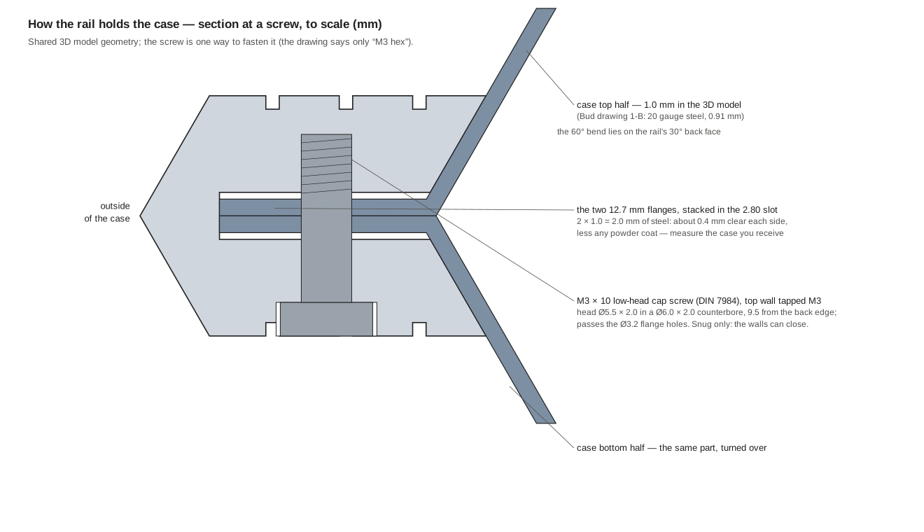
The case steel. Bud’s drawing 1-B calls for 20-gauge steel, 0.91 mm; the case model is 1.0 mm. Two flanges of 1.0 mm in a 2.80 mm slot leave about 0.4 mm on each side, less whatever paint or powder coat the case comes with. The slot is the loose part of this fit by design: Bud’s assembly drawing gives the slot as 3.0 ± 0.1 mm after assembly, opened slightly by the plugs pressed into its ends. Measure the two flanges together when the case arrives, before cutting the slot.
12.7.2 The stock
The finished section, 20.6 × 14.3 mm, fits inside a standard 5/8 × 1 in bar (15.88 × 25.4 mm) with 0.79 mm to remove from each flat face and 2.4 mm from each long edge. Speedy Metals lists 5/8 × 1 in 6061-T6511 aluminium flat (product 2289) in a 24 in length for $18.39, or cut to length by the inch (Speedy Metals, read 2 November 2026). One 24 in bar makes both rails: two blanks of about 272 mm (10¾ in) with room for the saw cut and squaring the ends. A 7/8 × 5/8 in bar would save metal, but it is not a common stock size.
T6511 is 6061-T6 that has been stretched after heat treatment to relieve internal stress. That matters for a long, thin part with a deep slot: stress-relieved bar moves much less when a slot opens it up, so the rail stays straight. Clear anodising, below, also suits 6061.
12.7.3 Closing the ends
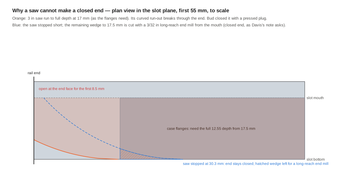
The note on Davis’s drawings, “Close ends via CNC milling — do not use plugs”, changes how the original was made. Bud’s own drawing 148 shows each extrusion with two plugs (item 2, part 1-S) pressed into the ends of the slot: “Gaps are permissible along areas indicated by (X’s) as plug must be interference fit.” The extrusion itself was open-ended, as an extrusion must be. The case agrees: each flange stops 17.5 mm short of the case’s front and back edges, which leaves room for the plugs.
That matters because a slitting saw, the natural tool for a long, deep, narrow slot, cannot leave a closed end. A saw cuts an arc. With a 3 in saw run to full depth where the flanges begin, 17.5 mm from the end, the arc carries on past the end of the rail: the end face is cut open for the first 8.5 mm of the slot’s depth.
There are three ways to finish the ends.
- Plugs, as Bud made it. Saw the slot right through, then press an aluminium plug into each end, 12 mm long, as deep as the slot and slightly thicker than it (Bud’s drawing gives 3.0 ± 0.1 mm across the slot after assembly, so start from 3 mm plate and sand to a firm press fit), with a drop of retaining compound, and face the end flush. This is the original construction. The seam will show faintly after anodising, which is presumably why Davis’s note, written for a CNC job shop, rules it out.
- Saw, then finish with an end mill. Stop the saw 30.3 mm from each end, so its arc leaves the end face whole, then clear the small wedge left at the bottom of the slot between 17.5 and 30.3 mm with a 3/32 in long-reach end mill working down from the mouth. The wedge is small, so this is a short job on either machine. The result is a closed end, as Davis’s note asks.
- End mill the whole slot. A 3/32 in end mill with at least 5/8 in of reach can cut the full slot, closed ends included, in two side-by-side passes. It is the cleanest result and the slowest: at about 0.1 mm per pass, 12.55 mm of depth is well over a hundred passes along each rail, with a slender cutter more than five diameters deep in a slot that must be kept clear of chips.
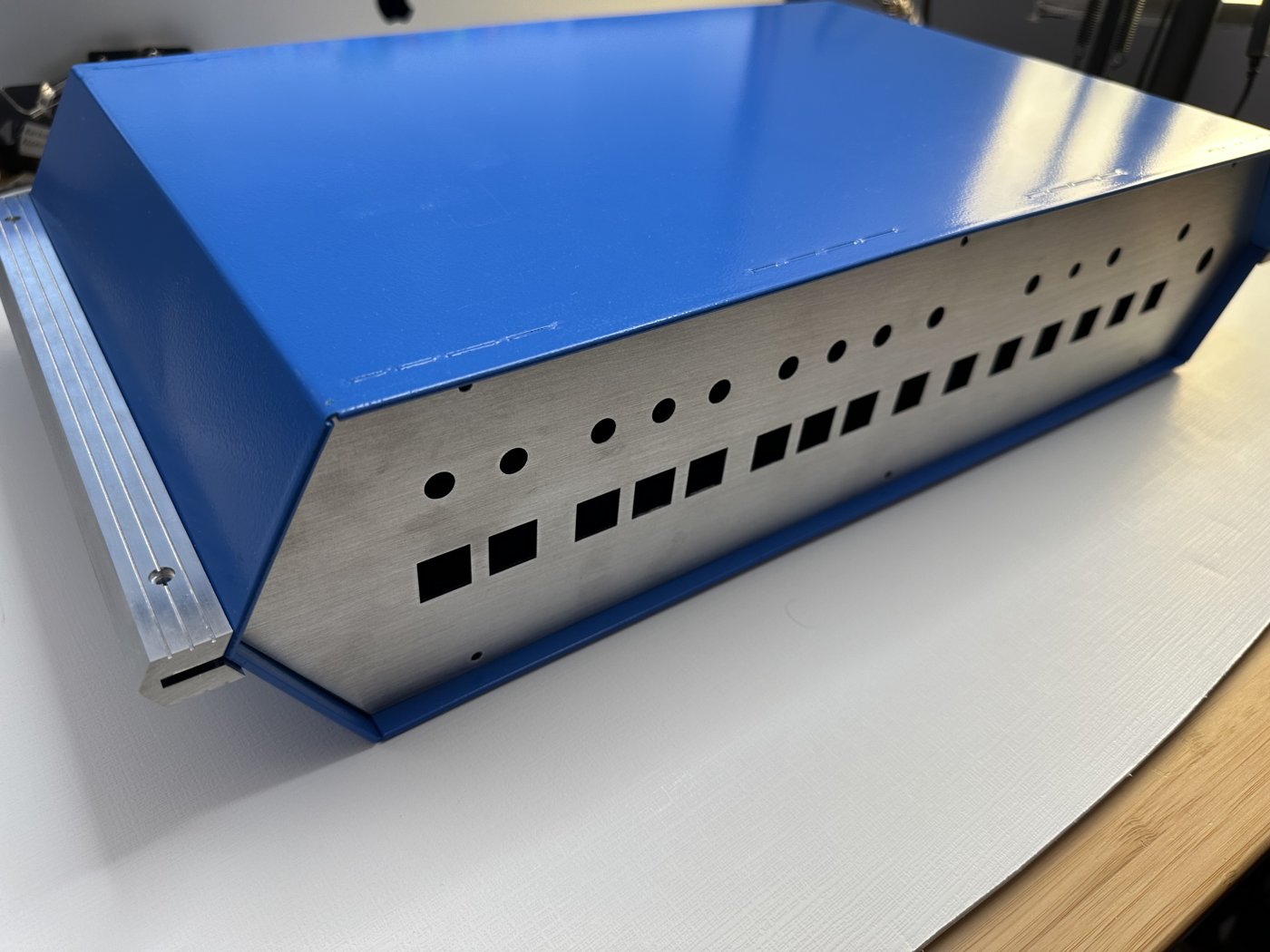
Kalinchuk’s PCBWay rails, in the photograph above, were left open at the ends despite the note, so an open end is evidently acceptable to the case. Option 2 gives the drawing’s closed ends at a fraction of the end-mill time and is the plan below. Option 1 is the faithful fallback if the wedge proves awkward.
12.7.4 Order of operations
The same order works on either machine, and it is chosen so that each operation has a flat, solid face to clamp on:
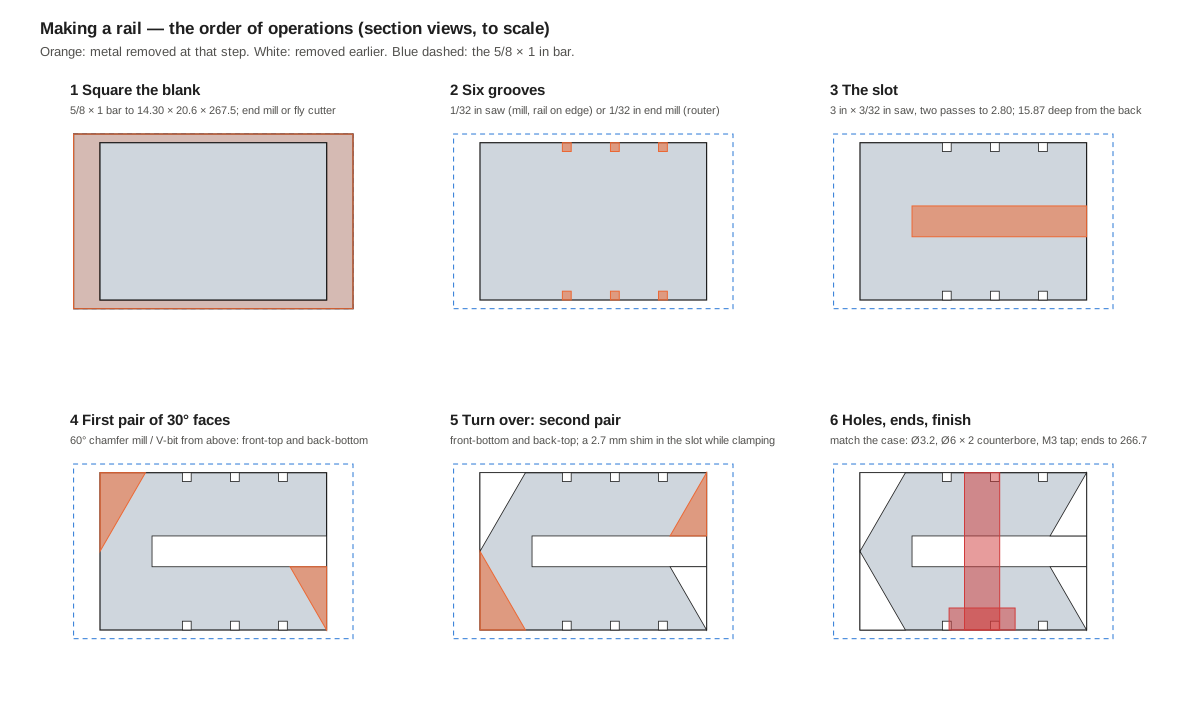
- Square the blank to 14.30 × 20.6 mm and about 267.5 mm long, leaving the ends a little long.
- Cut the grooves, three in each flat face, before anything weakens the bar.
- Cut the slot from the back edge, clamping on the solid strip in front of the slot’s bottom.
- Cut the first pair of 30° faces from above: the outer face on the top side and the inner face on the bottom side. Both face upwards when the rail lies flat.
- Turn the rail over and cut the other two. A strip of 2.7 mm shim stock in the slot stops the clamps from closing it.
- Drill, counterbore and tap to match the case, and finish the ends to 266.7 mm.
12.7.4.1 On the mini mill
The HiTorque 3990 has a 500 W brushless spindle variable from about 100 to 2,500 rpm, an R8 taper, a 460 × 120 mm table with three 12 mm T-slots, and 300 mm of X travel, enough to run the full rail past the cutter in one setting. Its head does not tilt, so every angle comes from the cutter or the fixture.
- Squaring. Hold the bar in the vise on parallels and take the 0.79 mm off each flat face with a 3/8 in three-flute carbide end mill or a fly cutter. Then stand it on edge to bring the width to 20.6 mm. The 272 mm blank is longer than the vise jaws, so support the overhang. Face the ends square with the side of the end mill, the bar overhanging the end of the vise.
- Grooves. Mount a 3 in × 1/32 in slitting saw (0.79 mm) on an R8 slitting-saw arbor, so that it cuts horizontally. Stand the blank on its front edge in the vise, gripped only about 6 mm deep: the grooves begin 7.5 mm up from that edge, so they are all above the jaws. Set each groove’s height on the Z axis, with the groove’s near edge at 3.57, 7.94 and 12.31 mm from the back edge (each groove 0.8 mm wide), and cut 0.8 mm deep in one pass along the full length. Turn the blank round to cut the other face.
- Slot. Change to a 3 in × 3/32 in (2.38 mm) saw. Lay the blank flat on a fixture plate bolted to the table, with its back edge flush with the plate’s edge and toe clamps on the solid front strip, the first 4.7 mm in front of where the slot will end. Cut the slot at mid-height in three depth steps of about 5.3 mm, to 15.87 mm from the back edge. Then raise the saw 0.42 mm and take a second pass to bring the slot to 2.80 mm. If a 7/64 in (2.78 mm) saw can be found, one pass does it. For a closed end, stop the saw 30.3 mm from each end (Option 2 above).
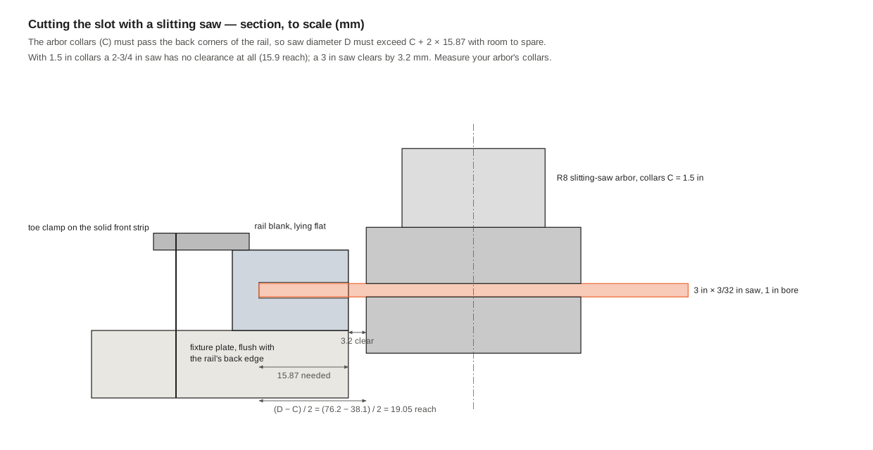
- Saw size. The arbor’s collars have to pass the rail’s back corners, because the slot’s bottom is 15.87 mm in from them. A saw of diameter D on collars of diameter C reaches (D − C) ÷ 2. With typical 1½ in collars, a 2¾ in saw reaches 15.9 mm, no clearance at all; a 3 in saw reaches 19.05 mm and clears by 3.2 mm. Measure the collars on the arbor actually used.
- The 30° faces. Use a 60° chamfer mill (60° included angle, each side 30° from the axis) at least ½ in across. With the rail lying flat, its flank lies on each 30° face. The face is 7.15 mm high and the flank of a ½ in tool about 10 mm, so each face is one cut, taken in light steps sideways. From above, it reaches the outer top face and the inner bottom face. Set the rail on parallels kept back from both edges, so the tool’s tip does not touch them. Turn the rail over, with the shim in the slot, for the other two faces. The point should meet at exactly 7.15 mm, mid-height: cut one side, measure, and set the second side from the first.
- End wedges (Option 2). Hold the rail on its edge, back up, and clear the wedge at each end from the mouth with a 3/32 in end mill with ⅝ in reach, in 0.1 mm steps. At the mill’s 2,500 rpm top speed, this small cutter works slowly but safely; it is also a natural job for the Shapeoko (below).
12.7.4.2 On the Shapeoko
The Shapeoko 3 XXL cuts aluminium with care: it is a belt-driven router on V-wheels, with a trim router turning 12,000 to 30,000 rpm (16,000 to 27,000 for a DeWalt DWP611) in 1/4 and 1/8 in collets. The machine in the Model Shop dive has had its stock belt-driven Z replaced by a lead screw, which stiffens the axis that matters most for metal. Its speed suits the small cutters this rail needs; its weakness is rigidity under heavier cuts.
- Squaring is best done on the mill even when the Shapeoko does the rest. On the router it means many light passes with a 1/8 in single-flute cutter.
- Fixture. Screw a fence of aluminium angle to the wasteboard and hold the rail against it with low toe clamps. Mark a registration stop at one end, so that the rail goes back in the same place after turning over. Set work zero by touching off on the fence corner.
- Grooves. Cut them with a 1/32 in two-flute carbide end mill, 0.8 mm deep in steps of about 0.1 mm, three per face. Turn the rail over against the fence for the other face.
- 30° faces. Use a 60° V-bit. A 1/4 in V-bit’s flank is only about 5.5 mm high against the 7.15 mm face, so cut each face in two or three steps: lower the bit and move it outward by the depth times tan 30° (0.577), and the flank stays in the same plane. Each step is a straight cut along the rail, so it is simplest to define the bit as a 60° chamfer tool and run a 3D contour over a model of the face (Fusion 360), or write the few moves by hand. A V-carve toolpath is the wrong tool for it.
- Slot (Option 3) or end wedges (Option 2). Stand the rail on its front edge in a V-block fixture, back up. The point is 120° included, so cut a matching vee into a hardwood or MDF block with the same 60° V-bit. Cut the slot or the wedges with a 3/32 in long-reach end mill working down from the mouth, with an air blast to clear the chips. Chips packed in a deep, narrow slot are what break small cutters.
The practical split, if both machines are used: square, groove, slot and face on the mill, where saws do the long cuts in a few passes, and take the rail to the Shapeoko for the closed-end wedges, which want a small cutter at router speed.
12.7.5 Cutters, speeds and feeds
LittleMachineShop, which sells the 3990, gives 165 surface feet per minute for milling wrought aluminium, 6061-T6 included (LMS cutting speeds). That is a conservative high-speed-steel figure, and it fits a small machine. Speed in rpm is SFM × 3.82 ÷ diameter in inches. For the router, the Shapeoko community wiki gives 1/8 in single-flute carbide in aluminium at about 15,000 rpm and 20–25 in/min with 0.05 in passes (Shapeoko wiki, Materials), and the usual community advice is a coated single-flute cutter, shallow passes and a chip load around 0.001 in per tooth. The miniature-cutter figures below are scaled down from that and are starting points, to be adjusted by sound and chip.
Table 13 — Cutters, speeds and feeds
| Operation | Cutter | Machine | Speed | Feed | Depth per pass |
|---|---|---|---|---|---|
| Squaring | 3/8 in 3-flute carbide (HSS: 1,700 rpm) | 3990 | 2,000–2,500 rpm | 150–200 mm/min | 0.5 mm side cut |
| Facing | fly cutter, 2 in swing | 3990 | about 300 rpm | 50–80 mm/min | 0.4 mm |
| Grooves | 3 in × 1/32 in HSS slitting saw | 3990 | about 210 rpm | 25–40 mm/min | 0.8 mm (full) |
| Slot | 3 in × 3/32 in HSS slitting saw | 3990 | about 210 rpm | 15–25 mm/min, by hand | about 5.3 mm, three steps |
| 30° faces | ½ in 60° chamfer mill | 3990 | 1,260 rpm HSS, up to 2,500 carbide | 80–120 mm/min | 0.5 mm |
| Holes | 2.5 and 3.2 mm drills; 6 mm 2-flute end mill | 3990 | 2,500 rpm | peck | counterbore 2.0 mm |
| Squaring (if routed) | 1/8 in single-flute carbide | Shapeoko | 15,000–18,000 rpm | 500–635 mm/min | 1.2 mm |
| Grooves | 1/32 in 2-flute carbide | Shapeoko | 18,000 rpm | 90–130 mm/min | 0.1 mm |
| Slot or end wedges | 3/32 in long-reach 2-flute carbide, ≥ ⅝ in reach | Shapeoko | 18,000 rpm | 150–180 mm/min | 0.1 mm |
| 30° faces | 1/4 in 60° V-bit | Shapeoko | 16,000–18,000 rpm | about 500 mm/min | 0.3 mm |
Saws and drills want cutting fluid; kerosene or WD-40 on aluminium is enough. Feed a slitting saw against its rotation (conventional), with the table gibs snug, because a saw that climbs into the work on a light machine grabs and breaks teeth. On the router, an air blast or mist matters more than any number in the table.
12.7.6 Holes and fasteners
Each rail has two holes, 23.85 mm from each end (219.0 mm apart), through both walls of the slot and through the two flanges inside it. Before drilling, put the case together and measure where the holes in its flanges actually are: their distance from the flange edge and from the case’s front and back edges. Then drill the rails to the case. The drawing’s 9.5 mm from the back edge is right for the case as modelled, but the case that arrives is the one that counts.
The fastening that fits the model’s counterbores is an M3 × 10 low-head cap screw, DIN 7984, from below:
- Drill 2.5 mm through both walls at each hole position.
- Open the bottom wall to 3.2 mm, and counterbore it Ø6.0 × 2.0 mm. The model’s 5.5 mm counterbore is exactly the screw head’s diameter, with no clearance.
- Tap the top wall M3 × 0.5. The screw engages about 3.5 mm of it, plenty for an M3 in 6061.
- An M3 × 10 screw, head flush in the counterbore, ends at 12.0 mm, inside the top wall.
Tighten the screws snug, not hard. The slot is wider than the flanges, so a hard pull bends the walls inward; the screw’s job is to locate the rail through the flange holes and keep it from sliding.
A set screw is the other common way to hold a rail of this kind: a tapped hole in one wall, with a cup-point set screw bearing on the flanges. If that route is chosen, note that a #6-32 screw (3.5 mm, 1/16 in hex key) will not pass the case’s 3.2 mm holes and can only press on the steel, while an M3 (1.5 mm key) can do either.
12.7.7 Deburring and finish
Break every edge with a fine file or a deburring tool, run a thin needle file along each groove and the slot’s mouth, and leave a small flat, about 0.2 mm, on the point. A knife-edge point takes anodising poorly and cuts fingers. Chase the M3 threads after finishing.
Bud’s drawing gives the finish as “etch and clear anodize.” The etch is a caustic dip that leaves a soft matte surface; the clear anodise seals it without colour. There are three ways to get close:
- Job-shop anodising. Ask for clear Type II sulphuric-acid anodise (MIL-PRF-8625 Type II, Class 1) with a caustic etch, or bead-blast first for the same matte look. Mask or plug the tapped holes. This matches the original most closely. Shops usually charge a minimum per lot, so send both rails together.
- Anodising at home with a hobby kit, if one is already in the shop: the same sulphuric-acid process at bench scale.
- Bead-blast or brush, then clear lacquer. Easiest, but the lacquer wears where hands touch the case.
The coating adds only thousandths of a millimetre, far below the slot’s clearance.
12.7.8 Checking the fit
Before the final finish, assemble the case dry and check each rail:
- The two flanges go fully into the slot, with the case’s 60° bends lying in the rail’s notch and no rocking.
- The rail’s ends are flush with the case’s front and back.
- A 3 mm drill shank passes through the rail and both flanges at each hole.
- The two rails stand parallel and the case closes square.
Bud’s drawing MD-1 says to fit the panels before the extrusions. A rail with plugged ends (Option 1) can slide on from the end before its plugs go in; a closed-end rail (Options 2 and 3) has to be pushed on sideways, flanges first, so check that the panels do not block it.
12.7.9 What the rails need
Table 14 — What the rails need
| Item | Specification | Source (examples) |
|---|---|---|
| Bar | 5/8 × 1 in 6061-T6511 aluminium, 24 in (both rails) | Speedy Metals product 2289 |
| Slitting saw, slot | 3 in diameter × 3/32 in (or 7/64 in) × 1 in bore, HSS | any machine-tool supplier |
| Slitting saw, grooves | 3 in × 1/32 in × 1 in bore, HSS | same |
| Saw arbor | R8 slitting-saw arbor, 1 in bore; check collar diameter | for example Grizzly H5621 |
| Chamfer mill | 60° included, ½ in body | — |
| End mills | 3/8 in 3-flute carbide; 6 mm 2-flute; 3/32 in long-reach, ⅝ in reach or more | — |
| Router cutters (if used) | 1/8 in single-flute; 1/32 in 2-flute; 1/4 in 60° V-bit | — |
| Drills and tap | 2.5 mm and 3.2 mm drills; M3 × 0.5 tap | — |
| Screws | M3 × 10 DIN 7984 low-head cap screws, 4 (plus spares) | — |
| Shim | 2.7 mm steel or aluminium strip, to support the slot while clamping | — |
| For Option 1 | 3 mm aluminium plate for four plugs; retaining compound | — |
12.8 Programming the Finished Machine
The front panel and the instruction set are described in Volume 6, and programming it from the panel in Volume 7, with games and longer programs in Volume 10. This section gives three things to do with a newly built machine, in order. Each program here was assembled and run in the series’ simulator, kenbak_sim.py, before being printed (03-outputs/tools/vol12_programs.py, which checks all three). The bytes are octal, as keyed.
12.8.1 Step 1: the factory checkout
The 1971 Installation and Maintenance manual (Library copy) gives a checkout that needs no program at all:
- Press and hold Start: the Run lamp lights. If it stays on when Start is released, press Stop.
- Press Display Address: the Address lamp lights.
- Press Clear: the Input lamp lights.
- Press Read Memory: the Memory lamp lights.
- Press Clear, then each of the eight data keys from the left. The lamp above each lights and stays lit. Clear puts all eight out.
This proves the keys, the lamps and much of the control logic. Step 5 also exercises chip 50: the data keys set bits in the INPUT byte at address 377, which is in that chip, and the lamps show it.
12.8.2 Step 2: the lamp test
Eighteen bytes. Set the address to 003 and store 004 there (the program counter), then key the bytes from 004:
004: 023 377 034 200 000 023 001 034
014: 200 223 000 203 001 243 017 311
024: 344 013
Table 15 — Step 2: the lamp test
| Address | Bytes | Instruction | What it does |
|---|---|---|---|
| 004 | 023 377 | LOAD A C=377 | all eight bits |
| 006 | 034 200 | STORE A OUTPUT | all eight data lamps on |
| 010 | 000 | HALT | look at them; press Start to go on |
| 011 | 023 001 | LOAD A C=001 | one bit |
| 013 | 034 200 | STORE A OUTPUT | light it |
| 015 | 223 000 | LOAD X C=000 | |
| 017 | 203 001 | ADD X C=001 | count X round 256 times, |
| 021 | 243 017 | JPD X≠0 017 | to make the step visible |
| 023 | 311 | ROTL A 1 | move the bit one place left |
| 024 | 344 013 | JPD UNC 013 | and again |
Press Start: all eight lamps light and the machine halts. Press Start again and a single light walks from bit 0 to bit 7 and round again. The simulator’s timing model, derived from the 1971 state descriptions rather than measured, puts each step at about 1.3 seconds on the original. A lamp that never lights is a lamp, its wiring or its 7416. A lamp that lights with its neighbour is a short.
12.8.3 Step 3: the memory tests
A KENBAK-1 holds its registers in memory, so a machine with a bad 1404A can fail in confusing ways. Two programs separate the chips. MEMTEST1 lives in chip 59 (delay line 0) and tests chip 50. MEMTEST0 is the same program assembled to live in chip 50 and test chip 59. Each fills its test area with a pattern (each byte equal to its offset), reads it back, then repeats with the complement of the pattern, so that every bit of every location is tried as both 0 and 1. Each clean pass adds one to a count in the lamps. On the first mismatch the program halts with the failing address in the lamps.
MEMTEST1: P (address 003) = 004. It tests 204 to 376, leaving alone the OUTPUT byte at 200, the overflow and carry bytes at 201–203 and the INPUT byte at 377.
004: 123 000 134 200 223 000 024 002
014: 036 204 203 001 024 002 013 173
024: 043 012 223 000 026 204 014 002
034: 043 116 203 001 024 002 013 173
044: 043 030 223 000 023 377 014 002
054: 036 204 203 001 024 002 013 173
064: 043 050 223 000 023 377 014 002
074: 016 204 043 116 203 001 024 002
104: 013 173 043 070 103 001 134 200
114: 344 010 024 002 003 204 034 200
124: 000MEMTEST0: P (address 003) = 204. It tests 004 to 177. Chip 59 also holds the registers at 000 to 003, which the program itself uses, so a fault there shows up as a machine that will not run at all rather than as an address.
204: 123 000 134 200 223 000 024 002
214: 036 004 203 001 024 002 013 174
224: 043 212 223 000 026 004 014 002
234: 043 316 203 001 024 002 013 174
244: 043 230 223 000 023 377 014 002
254: 036 004 203 001 024 002 013 174
264: 043 250 223 000 023 377 014 002
274: 016 004 043 316 203 001 024 002
304: 013 174 043 270 103 001 134 200
314: 344 210 024 002 003 004 034 200
324: 000
The structure, in the assembler notation of Volume 7 (MEMTEST1’s addresses):
Table 16 — The structure, in the assembler notation of Volume 7 (MEMTEST1's addresses)
| Address | Label | Instruction | Notes |
|---|---|---|---|
| 004 | START | LOAD B C=000 / STORE B OUTPUT | pass counter, shown in the lamps |
| 010 | LOOP | LOAD X C=000 | X is the offset into the test area |
| 012 | FILL | LOAD A X / STORE A 204,X / ADD X C=001 / LOAD A X / SUB A C=173 / JPD A≠0 FILL | write the offset into every location (173 octal = 123 locations) |
| 030 | CHK | LOAD A 204,X / SUB A X / JPD A≠0 FAIL … | read it back |
| 050 | FILL2 | LOAD A C=377 / SUB A X / STORE A 204,X … | write the complement, 377 − offset |
| 070 | CHK2 | LOAD A C=377 / SUB A X / SUB A 204,X / JPD A≠0 FAIL … | read it back |
| 110 | ADD B C=001 / STORE B OUTPUT / JPD UNC LOOP | count a clean pass | |
| 116 | FAIL | LOAD A X / ADD A C=204 / STORE A OUTPUT / HALT | lamps = the failing address |
In the simulator, both tests count passes on good memory, about five seconds a pass in the timing model. With a bit deliberately stuck at 0, at address 250 for MEMTEST1 and 050 for MEMTEST0, each halts with that address in the lamps. Run MEMTEST1 first: it needs chip 59 working only well enough to hold the program and registers, and it says whether chip 50 is good. Then run MEMTEST0. If one chip fails, swap the two 1404As. If the fault moves with the chip, the chip is bad; if it stays, look at that chip’s input and output gating on sheet 24, its pull-up and pull-down resistors, or its socket. This is the test for the two spare 1404As, too.
12.9 Still Open
- The board in the hand: my board arrived on 4 November 2026, and its memory positions are DIP-8 with the square pad at pin 1, as the files show. Still to do: find the holes for C9, C14 and C15 on the board (marked ≈ on the assembly drawing).
- R15: 1 kΩ or 3 kΩ; it will be socketed until the machine says which.
- Lamps: the Tayda A-6044 holders and built-in-resistor LEDs, to be checked in my panel’s 5.9 mm holes.
- Heat: whether chip heat sinks or a fan are needed, measured after an hour in the closed case.
12.10 Printable Bill of Materials
The whole parts list above is also a printable PDF for the bench: KENBAK-1 full-size BOM (PDF). Each part has a row with tick boxes for ordered, in hand and fitted, the quantity and reference designators, the part number to buy, alternates (every obsolete part names one, or says there is none), where to buy it, its tag and space for notes. The last page is an order log.
12.10.1 Where every part goes: the assembly drawing
The bare board has no printed legend, only the chip numbers etched in its copper, and the optional kenbak.com silkscreen prints its designators so small, and mostly upside down, that they are hard to read. So the board’s component side is redrawn here with every part labelled upright: the designator in the BOM’s numbering (IC, R, C, CR, Q), the chip type or value, and a one-inch grid lettered A to R and numbered 1 to 10. Click the drawing to open it as a PDF in a new tab. Sheet 1 is the whole board; sheets 2 to 7 are its six parts enlarged to a readable size for printing on letter paper; the last two sheets are a parts index giving each designator’s type or value, grid square and sheet, with a box to tick when it is fitted.
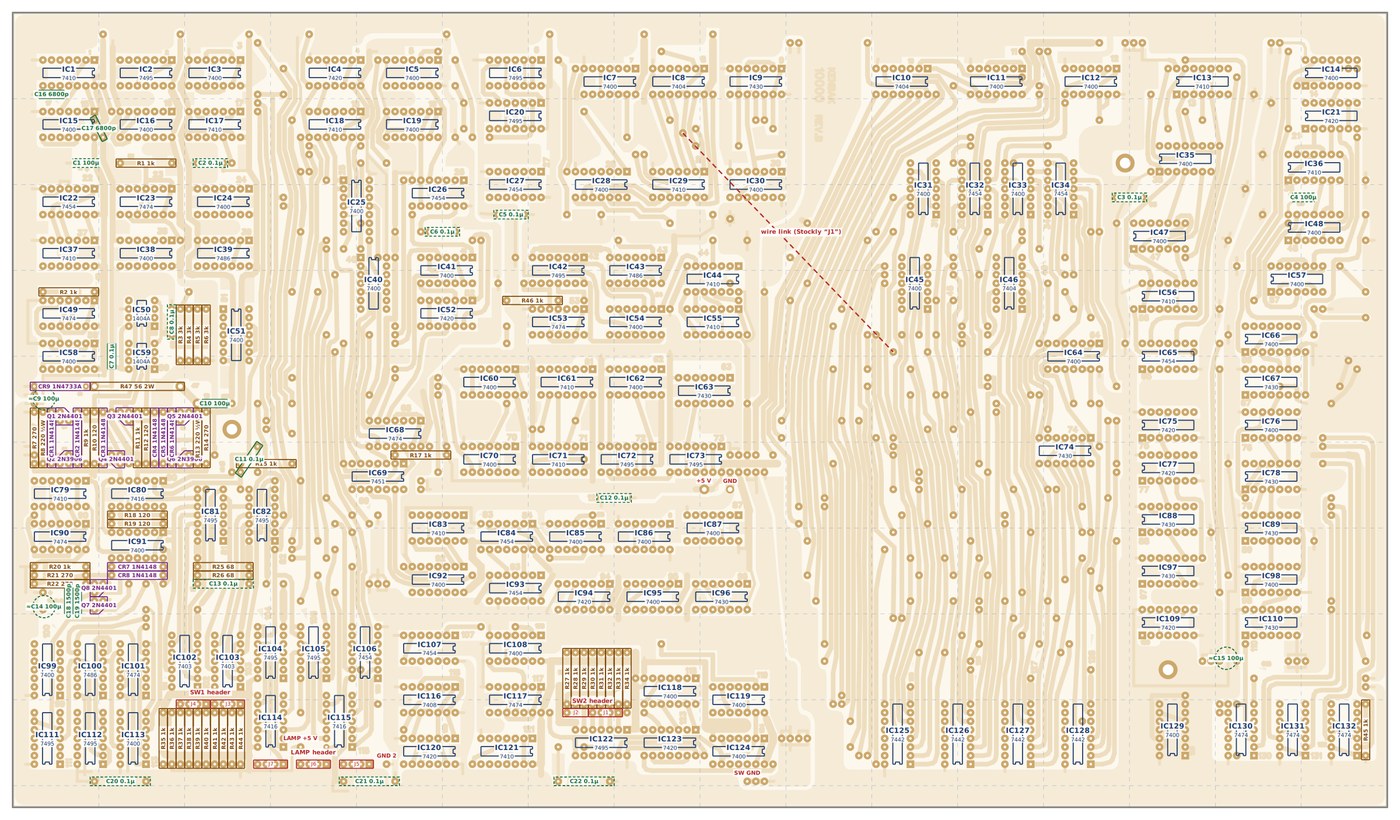
KENBAK-1 board assembly drawing (PDF, 9 sheets, letter landscape). The drawing, drawn for this series from the kenbak.com Gerbers and silkscreen (Library copy), with chip types and the capacitors the silkscreen leaves out taken from Stockly’s 2007 parts-placement guide (Library copy).
The drawing follows the board’s own files, with three points to check against the board itself:
- Fourteen capacitors are not on the kenbak.com silkscreen: C1 to C6, C8, C9, C12 to C15 and C20 to C22. Their places come from Stockly’s drawing of the same board and are drawn dashed, in italics. Eleven match a pair of holes on the board exactly. C9, C14 and C15 are electrolytics among holes that the 2007 drawing does not separate, so they are marked ≈ and circled: find their holes from the copper, with + to the supply side, before soldering.
- The connector names (SW1, SW2, LAMP, +5 V, GND) are Stockly’s; the silkscreen splits the same headers into J1 to J7. The BOM’s J1 is Stockly’s insulated wire link, drawn as a dashed line.
- C16 and C17 go on the underside, as in the BOM. R16, R23 and R24 are not fitted on this board.
Next — Volume 13: My µKENBAK-1. The full-size board is a waiting game for parts; the half-scale µKENBAK-1 from Adwater & Stir runs the same instruction set on a microcontroller and can be built in an evening, its schematic, firmware and parts list laid out the same way.
Footnotes
-
kenbak.com, “Making a Reproduction”: parts list, power measurements, substitutions and build notes, https://www.kenbak.com/reproduction (read 2 November 2026; Library copy). ↩ ↩2 ↩3 ↩4
-
Texas Instruments product pages, read 2 November 2026: https://www.ti.com/product/SN7400, https://www.ti.com/product/SN7404 and https://www.ti.com/product/SN7416 list active orderable parts; the pages for SN7403, SN7408, SN7410, SN7420, SN7430, SN7442A, SN7451, SN7454, SN7474, SN7486 and SN7495A return “not found”. ↩
-
Mean Well, RT-65 series specification (RT-65A to RT-65D), https://www.meanwell.com/Upload/PDF/RT-65/RT-65-SPEC.PDF. ↩
Comments (0)