KENBAK-1 · Volume 13
KENBAK-1 — Volume 13 — My µKENBAK-1
The half-scale Adwater & Stir kit as a reference for my own build: the circuit drawn out pin by pin, the board and where every part goes, a complete parts list with current replacements, the firmware and its extensions, loading programs over USB, rebuilding the firmware, and a table of faults and fixes
13.1 About This Volume
I have ordered Adwater & Stir’s µKENBAK-1 kit, and I am on the waiting list for its pocket-sized sibling, the nanoKENBAK-1, which is sold out. I am building the µKENBAK-1 alongside the full-size TTL reproduction that began in Volume 11. This volume is about the µKENBAK-1. The nanoKENBAK-1 has the next volume to itself.
Volume 9 has already set out the kit’s assembly in the maker’s order, from the lamps and keys aligned against the front panel through to the key caps and rubber feet, with the maker’s addendum and an acceptance test for the firmware. That procedure is not repeated here. This volume holds what Volume 9 left out, and what a builder needs once the kit is together, or when it goes wrong:
- the circuit, drawn out pin by pin, because the maker publishes no schematic;
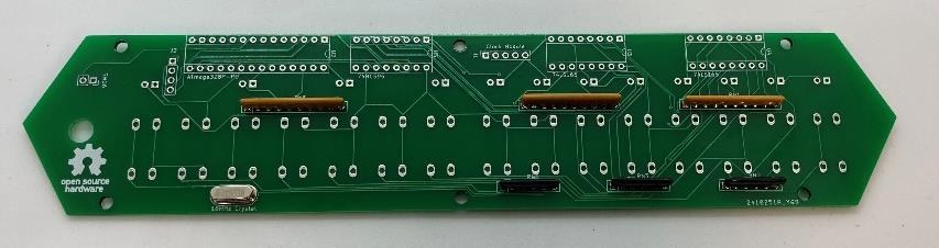
- the board, photographed bare and populated, with a map of where every part goes;
- a complete parts list in the form used in this site’s clock builds: every part, what to buy now to replace it, and why;
- the firmware: Mark Wilson’s Kenbak-uino, what it adds to the 1971 machine, and how the kit’s build differs from the published source;
- programming from the keys, over USB, and from the processor’s own EEPROM, with a tool written for the series that makes and checks load files;
- rebuilding the firmware, with the one change the kit needs;
- faults and fixes.
Everything in this volume comes from the maker’s published booklets and pages (Library copies: assembly booklet V2.5, operations booklet V2.5, assembly booklet V2), from Wilson’s source code, and from the data sheets of the parts (Library copies: ATmega328P, 74HC165, 74HC595, DS3231). The French magazine Programmez! reviewed the kit (Library copy). Where something is inferred rather than read from a source, it says so.
13.2 The Machine in One Table
Table 1 — The Machine in One Table
| µKENBAK-1 version 2.5 | |
|---|---|
| Maker | Adwater & Stir (Chris Davis, Famous Davis LLC, Willmar, Minnesota) |
| Scale | half size; steel case with milled aluminium ends, brushed-aluminium front panel |
| Processor | Microchip (Atmel) ATmega328P, 28-pin DIP, in a socket |
| Clock | 16 MHz crystal |
| KENBAK-1 memory | 256 bytes, held in the processor’s 2 KB of RAM |
| Program storage | the processor’s 1 KB EEPROM, eight “pages” |
| Panel | 8 white data lamps, 4 yellow control lamps, 15 keys, power toggle |
| Lamp drive | one 74HC595 shift register (data lamps); four processor pins (control lamps) |
| Key input | two 74HC165 shift registers in a chain |
| Real-time clock | DS3231 module on a five-pin header |
| Host link and power | USB-to-serial module, micro-USB, brought to the case wall by a short extension |
| Firmware | Mark Wilson’s Kenbak-uino (MIT licence), pre-programmed |
| Price | $124.95 kit, $174.95 built and tested (product pages, 27 October 2026) |
13.3 The Circuit
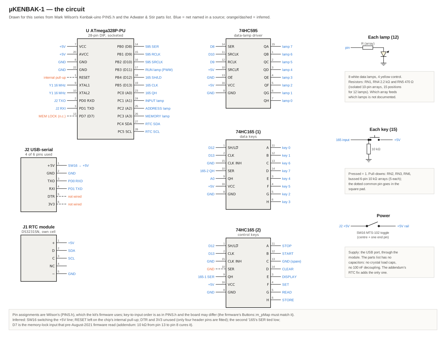
Adwater & Stir does not publish a schematic of the µKENBAK-1. It does not need one, because the circuit is Mark Wilson’s. When Wilson built his Kenbak-uino in 2011 he drew its schematic in plain text inside the firmware itself, in the file PINS.h, and the kit runs that firmware. The pins the firmware drives fix the wiring: a board wired any other way would not work with it. The drawing below is made from PINS.h (as corrected by Wilson in May 2025), the booklet’s parts list and designators, and the pin numbers in the data sheets (Kenbakuino on GitHub).
13.3.1 Power
There is no regulator, no battery and no mains supply. The machine runs from the 5 V of the USB port, taken from the +5V pin of the USB-to-serial module, through the toggle switch SW16, to the board’s supply rail. The booklet says only that a wire goes from the SW16 pads to the switch’s centre and bottom pins; that the switch interrupts the +5 V line, rather than some other connection, is the obvious reading but is an inference. The whole machine draws little enough for any USB port: one microcontroller, three logic chips, a clock chip and at most twelve lamps.
The booklet’s parts list contains no capacitors at all: no load capacitors for the crystal and no 100 nF decoupling capacitors beside the chips, which most designs would treat as compulsory. The circuit works without them, as the kits in use show, but it explains the one fault in the addendum that is cured by adding a capacitor (the clock that forgets the time, below), and it is why the parts list in this volume offers two optional capacitors.
13.3.2 The processor
The ATmega328P is the processor of the Arduino Uno, running at 16 MHz from crystal Y1. The KENBAK-1’s 256 bytes of memory, its registers (which on the KENBAK-1 are simply memory locations 000 to 003) and its whole control logic are in the firmware. Pins 7 and 20 take +5 V, pins 8 and 22 ground. The serial pins, PD0 (pin 2) and PD1 (pin 3), go to the module’s TXO and RXI. Its RESET pin (pin 1) is not connected to anything in any source, so it is presumably left on the chip’s internal pull-up resistor, which is enough to hold it high in normal use.
13.3.3 The data lamps
The eight data lamps hang on one 74HC595, a serial-in, parallel-out shift register with an output latch. The processor clocks a byte into it on three wires (data on D8, shift clock on D10, latch on D9), then pulses the latch, and all eight lamps change at once. The ‘595’s output-enable is tied low and its clear high, so it is always on. One detail is worth knowing for repairs: the ‘595’s first output, QA, drives the leftmost lamp, bit 7, and its last, QH, drives bit 0. Wilson notes this in PINS.h (“Note the order!”) because the obvious assumption, QA = bit 0, is wrong; the firmware shifts the byte out least-significant bit first to match. A board with a bad ‘595 output therefore shows a dark lamp at the opposite end from where a naïve probe would look.
The four control lamps (Input, Address, Memory, Run) are driven straight from processor pins: A1, A2 and A3 for the first three, and D11 for Run. D11 can be pulse-width modulated, which is how the firmware dims the Run lamp to imitate the original’s flicker while a program runs, and how the SysInfo call 020 sets its brightness.
Each lamp has a series resistor to ground. The kit supplies these as three 10-pin resistor arrays of five independent resistors each: two of 2.2 kΩ (marked 10X-2-222LF) in RN1 and RN4, and one of 470 Ω (10X-2-471LF) in RN5, fifteen positions for twelve lamps. The booklet does not say which array feeds which lamps. The values suggest the arrangement: 2.2 kΩ is plenty for a modern white LED, which is bright at a milliamp, and 470 Ω suits the yellow LEDs, which need more current for the same brightness. Wilson’s own build used 220 Ω throughout.
13.3.4 The keys
The fifteen keys are read by two 74HC165 parallel-in, serial-out shift registers chained together: the second ‘165’s output feeds the first one’s serial input, so the processor sees one sixteen-bit stream on a single pin (A0). To read the panel, the firmware pulls the shared SH/LD line (D12) low and high again, which copies all sixteen key states into the registers at once, then clocks them out on D13. Each key connects its ‘165 input to +5 V when pressed, and a 10 kΩ resistor holds the input low otherwise; the kit’s three bussed 6-pin arrays, RN2, RN3 and RN6, supply the fifteen pull-downs, five each. Because they are bussed (one common pin, marked with a dot), they must go in the right way round, dot to the square pad.
The order is not the panel’s order. In Wilson’s wiring the first ‘165 carries the data keys in the order 0, 1, 6, 7, 4, 5, 2, 3, and the second carries Stop, Start, an unused input tied to ground, Clear, Display, Set, Read and Store; a table in the firmware, Buttons::m_pMap, puts them back in order. That makes no difference to a builder, because the board is made, but it matters to anyone tracing a key that does not work: data key 2 is on pin G of the first ‘165, not pin C.
13.3.5 The clock and the serial port
The real-time clock is a ready-made DS3231 module plugged into the five-pin header J1 (+, data, clock, unused, ground). It talks to the processor on the I²C bus (SDA on A4, SCL on A5) and has its own backup cell, so it keeps time when the machine is off. The firmware reads it only when asked: by the three clock programs, and by any program that uses the SysInfo call.
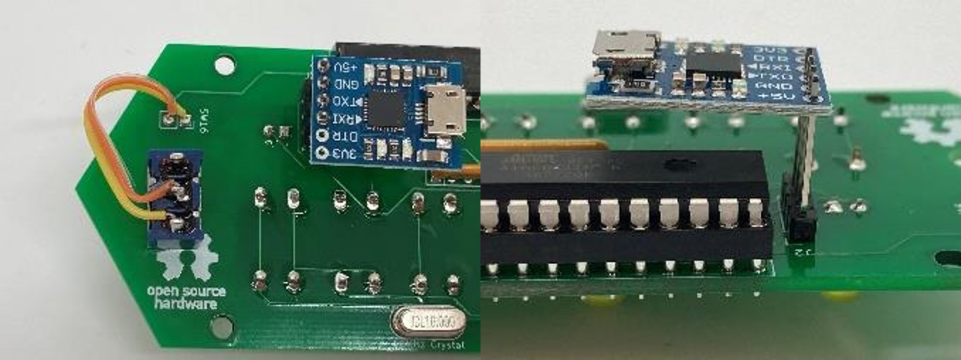
The USB-to-serial module on J2 gives the machine both its power and its serial port. The module photographed in the booklet has six pins (+5V, GND, TXO, RXI, DTR, 3V3), and only the first four are used. That matters for programming. An Arduino board resets its processor through the DTR line whenever a computer opens the port, which is how the Arduino software uploads new firmware without a button press. With DTR not connected, the µKENBAK-1 cannot be reprogrammed through its USB socket as it stands, which is why the maker’s method is to move the chip to an Arduino Uno (below).
13.3.6 The memory-lock pin
One pin more appears in the drawing, in orange: D7, pin 13. The maker’s addendum explains it. Kits bought before 24 August 2021 had firmware that read a memory-lock switch, the µKENBAK-1 has no such switch, and the floating input sometimes read as “locked”, so that Store did nothing. Wilson’s published source has no lock input at all, so the kit’s firmware was evidently built from a modified copy of it. Later kits do not read the pin; earlier ones can be cured with a resistor (see the faults table).
13.4 The Board
The board is a single two-layer printed circuit board, pointed at both ends to fit the case, green, with the lamps and keys on the front face and everything else on the back, “the side with the ‘Open Source Hardware’ logo”. Every chip is in a socket. Laid out from the left as seen from the back, the top row holds the USB module position J2, the power-switch pads SW16, the ATmega328P, the 74HC595, the clock-module header J1 and the two 74HC165s; below them run the three yellow 10-pin resistor arrays, the rows of key and lamp pads, the crystal and the three black 6-pin arrays.
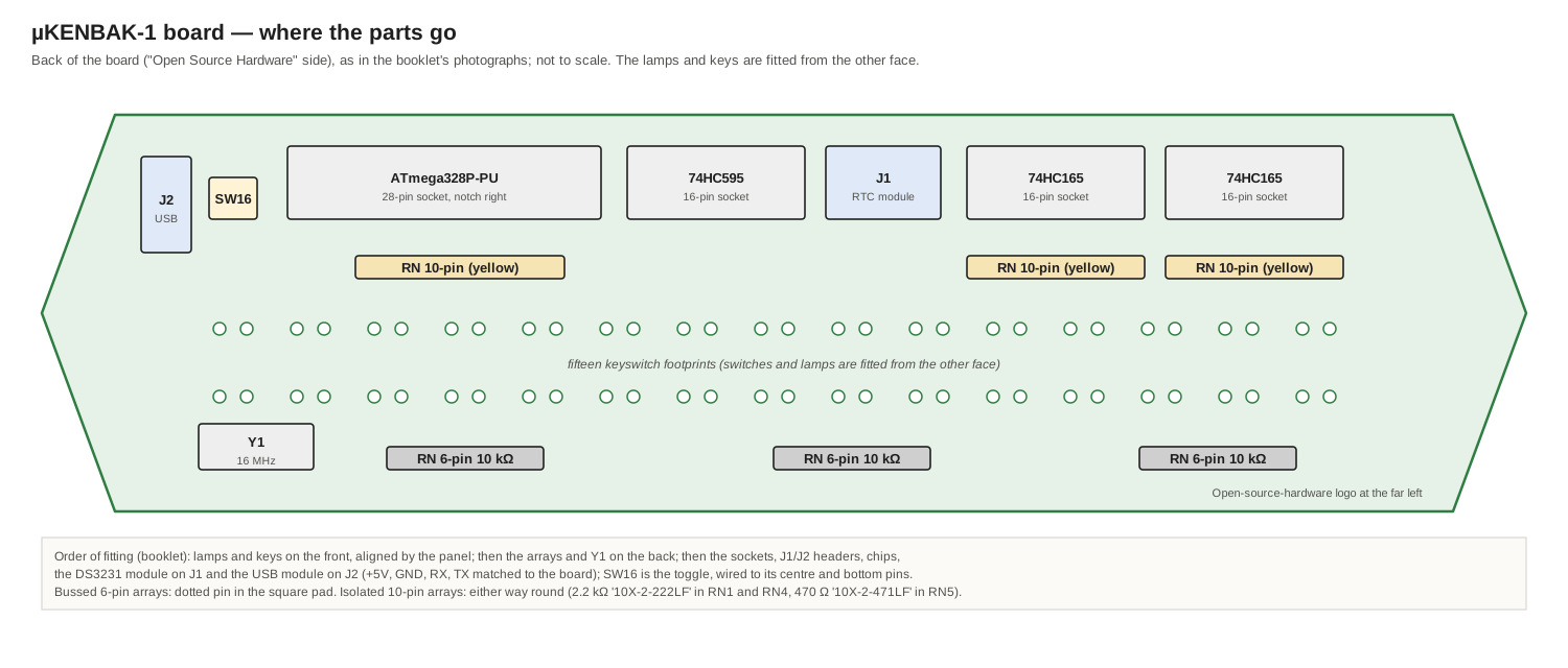
The silk screen labels the two key chips 74LS165, the booklet’s parts list calls them 74HC165, and its step text calls the shift registers 74LS165 and 74LS595. The parts in the photographs are marked 74HC. Either family works at 5 V with these inputs; buy HC (parts list below).
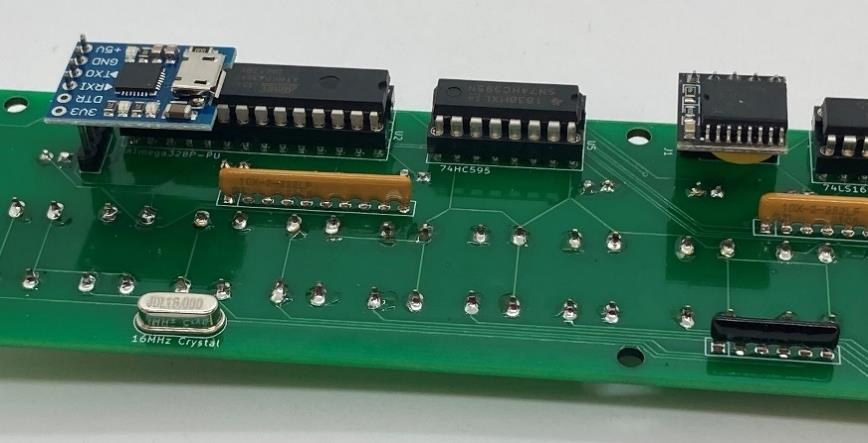
Two parts are modules rather than components, and both deserve a look before they are soldered:
- The USB-to-serial module is the common blue board with a micro-USB socket and six pins. The booklet tells builders to install the “CH-340 serial drivers”, but the module in its photographs carries a square QFN chip of the kind found on CP2102 modules, and makers of these boards change chips without changing the board’s look. Linux has drivers for both built in; on other systems, the chip’s marking says which driver to install. More important is the pin order: J2’s four pads are +5V, GND, RX and TX, the module’s first four pins are +5V, GND, TXO and RXI, and the module stands on the four-pin header so that they meet. A replacement module with a different pin order must be wired, not plugged.
- The DS3231 module is a small black board with the DS3231SN chip on top and a coin cell underneath, made to plug onto a Raspberry Pi’s first five header pins, which is why its pins run +, D, C, NC, −. It goes on J1 in the orientation shown in the booklet; turned round, it would put +5 V on its ground pin.
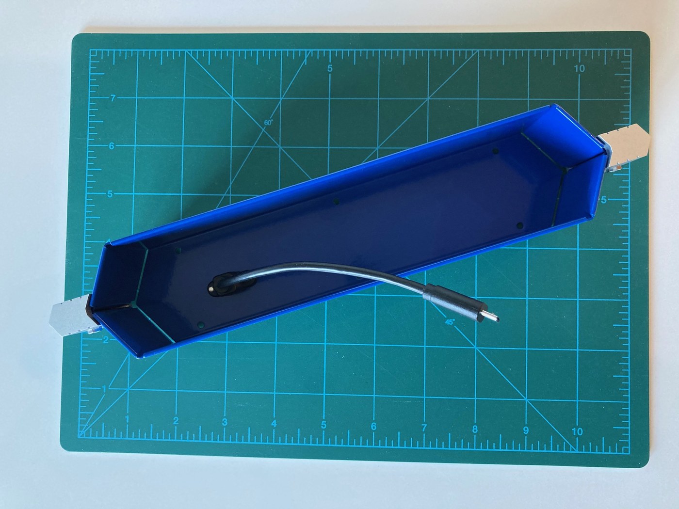
The case is two folded steel halves, with the board and panel screwed in on 40 mm nylon standoffs, a short micro-USB extension from the module to a socket in the case wall, and milled aluminium ends held by flat-head screws into brass knurled nuts. Nothing inside the case is fixed to the board except by those screws, so the board comes out in a few minutes for repair.
13.5 Bill of Materials
The kit supplies everything, so this list is for spares, repairs and anyone building a second board from a bare one. It starts from the booklet’s parts list (rev. 2.5) and gives, for every line, the part supplied, the part to buy now, and why it changed. The tags follow the clock volumes on this site:
Table 2 — The kit supplies everything, so this list is for spares, repairs and anyone building a second board from a bare one. It starts from the booklet's parts list (rev. 2.5) and gives, for every line, the part supplied, the part to buy now, and why it changed. The tags follow the clock volumes on this site
| Tag | Meaning |
|---|---|
| Same | The supplied part is still a standard catalogue item; buy it as listed |
| EOL | The supplied part is obsolete or no longer the usual one; a replacement is needed |
| Spec | The parts list does not say enough to buy it (no value, rating or part number), or the part needs a check |
| Conflict | The parts list, the board and the photographs disagree |
| Choice | A change or addition chosen for this build, not in the kit |
Prices and stock change daily, so none are given; part numbers are examples that meet the specification. A printable version with tick boxes is at the end of this volume (Printable Bill of Materials).
13.5.1 Semiconductors and modules
Table 3 — Semiconductors and modules
| Qty | Where | Supplied | Buy now | Tag | Why |
|---|---|---|---|---|---|
| 1 | U, 28-pin socket | ATmega328P, pre-programmed | ATmega328P-PU (Microchip, 28-pin DIP), with the Arduino Uno bootloader already burned, or burn it yourself | Spec | The chip is current, but a blank one runs nothing: it needs the firmware, and the maker’s reprogramming method (an Uno) needs the Uno bootloader too. Not the ATmega328-PU (no P), which has a different signature and needs a changed board definition. Keep the original chip as the master |
| 1 | 16-pin socket | 74HC595 | TI SN74HC595N | Same | Active part1 |
| 2 | 16-pin sockets | 74HC165 (silk screen and step text: 74LS165) | TI SN74HC165N | Conflict | The parts list and the chips in the photographs are HC; the board’s silk screen says LS. HC is the right family for a 5 V microcontroller design and is what the firmware’s timing was written with2 |
| 1 | J1 | DS3231 RTC module, 5-pin (+, D, C, NC, −) | A DS3231 module with the Raspberry Pi 5-pin pinout | Spec | Clock modules come in many pinouts; this one must match J1’s order. The large ZS-042 type (DS3231 with a 24C32 EEPROM) has a different pinout and does not fit. Check the backup cell’s marking before replacing it: some modules are built for a rechargeable cell and some for a primary one |
| 1 | J2 | USB-to-UART TTL module, micro-USB, 6-pin | 6-pin CP2102 or CH340 micro-USB module, 5 V type, pins in the order +5V, GND, TXO, RXI, DTR, 3V3 | Spec | The parts list gives no chip or pinout; the booklet’s text names the CH340, its photographs show a QFN chip like a CP2102. Any 5 V module with this pin order drops in; another order must be wired by hand |
| 12 | Front, lamps | 8 × white, 4 × yellow 5 mm LED | 5 mm LEDs, diffused or clear to taste, white and yellow | Same | Match the long-lead-right orientation (Volume 9). Brightness differs between makers; buy all eight data lamps from one batch so they match |
13.5.2 Passive parts
Table 4 — Passive parts
| Qty | Where | Supplied | Buy now | Tag | Why |
|---|---|---|---|---|---|
| 2 | RN1, RN4, lamp resistors | 2.2 kΩ isolated array, 10-pin, marked 10X-2-222LF | Bourns 4610X-102-222LF | Same | The marking is Bourns’ 4600X series: 10 pins, five isolated 2.2 kΩ resistors3. Either way round |
| 1 | RN5, lamp resistors | 470 Ω isolated array, 10-pin, marked 10X-2-471LF | Bourns 4610X-102-471LF | Same | As above, 470 Ω |
| 3 | RN2, RN3, RN6, key pull-downs | 10 kΩ bussed array, 6-pin, black | Bourns 4606X-101-103LF | Same | Five 10 kΩ resistors to one common pin; the dotted common pin goes in the square pad |
| 1 | Y1 | 16 MHz crystal | 16 MHz quartz crystal, HC-49/US | Same | The board has no load capacitors, so the crystal runs on the stray capacitance of the board and the chip; a standard 18–20 pF crystal is what the kit uses |
| 1 | Across the RTC module’s + and − pins | (addendum fix, not in the kit) | 0.1 µF, 50 V, X7R ceramic | Conflict | The addendum says “.01uF (104)”; a 104 marking is 0.1 µF, not 0.01 µF. Either works as decoupling; fit only if the clock resets to 12:00 at power-on |
| 1 | Across ATmega pins 7 (VCC) and 8 (GND), underneath | (none) | 0.1 µF, 50 V, X7R ceramic, short leads | Choice | Optional. The kit has no decoupling at all; pins 7 and 8 are adjacent, so a capacitor soldered across them on the back is the classic retrofit. Not required: kits run without it |
| 1 | D7 (pin 13) to ground (pin 8) | (addendum fix) | 10 kΩ, ¼ W | Same | Only for kits bought before 24 August 2021 whose Store key sometimes does nothing |
13.5.3 Panel and switches
Table 5 — Panel and switches
| Qty | Where | Supplied | Buy now | Tag | Why |
|---|---|---|---|---|---|
| 15 | Keys | tactile push-button, through-hole | 12 × 12 mm through-hole tactile switch with the square stem that takes the kit’s caps | Spec | The parts list says only “tactile push button”. The photographs show 12 mm switches with square stems. Match the stem to the cap before buying; the caps must not bind (Volume 9) |
| 15 | Key caps | 8 black, 7 white square caps | Spares from Adwater & Stir | Same | The caps match the case’s panel holes; generic 12 mm caps vary in size |
| 1 | SW16, power | MTS-102 miniature toggle | MTS-102 (SPDT on-on, 6 mm bushing) | Same | Two of its three pins are used |
| 1 | Front panel | screen-printed brushed aluminium | Adwater & Stir only | Same | Made for the kit |
13.5.4 Case and hardware
Table 6 — Case and hardware
| Qty | Where | Supplied | Buy now | Tag | Why |
|---|---|---|---|---|---|
| 1 | Case | steel, two folded halves | Adwater & Stir only | Same | |
| 2 | Ends | milled aluminium | Adwater & Stir only | Same | Masking tape under a loose end, per the booklet |
| 6 | Panel standoffs | 40 mm female-female hex, nylon | M3 × 40 mm nylon hex standoffs, female-female | Same | |
| 6 / 6 / 4 | Screws | 12 mm and 8 mm pan-head; 14 mm flat-head | M3 pan-head 12 mm and 8 mm; M3 flat-head 14 mm | Spec | The parts list gives lengths, not threads; the USB extension is fixed with “M3 bolts”, so the kit’s hardware is metric. Check one supplied screw before buying |
| 4 | End fixings | M3 knurled nuts (brass) | M3 brass knurled nuts | Same | |
| 6 | Spacers | 4 mm white nylon | 4 mm nylon spacers, M3 clearance | Same | Hold the panel off the LEDs during soldering |
| 1 | USB to case wall | USB extension | Panel-mount micro-USB extension, male to female, with two M3 screw ears | Spec | The socket must be the type the case wall is cut for; the one supplied has two screw ears either side |
| 1 | Header | 5-pin male | 2.54 mm pin header | Same | J1 |
| 1 | Header | 4-pin male, 19 mm | long-pin 2.54 mm header, about 19 mm overall | Same | J2, holds the USB module clear of the ATmega |
| 3 / 1 | Sockets | 16-pin and 28-pin DIP | 16-pin and 28-pin narrow (0.3 in) machined (turned-pin) DIP sockets | Choice | The ATmega328P is a narrow DIP. I use only machined sockets; fit them in place of any stamped sockets in the kit |
| 4 | Feet | rubber | self-adhesive rubber feet | Same | |
| 1 | USB cable | (not supplied) | USB-A to micro-USB data cable | Spec | Many micro-USB cables carry power only. A charge-only cable lights the machine but no serial port appears on the computer |
13.6 Before the First Power-Up: Five Minutes With a Meter
Volume 9 stops for a first power-up before the case goes on. Five checks with a multimeter, made with the chips out of their sockets, catch the faults that can damage parts:
- +5 V to ground across the 28-pin socket, pin 7 to pin 8: it should read high (kilohms or more), not near zero. A short here is a solder bridge.
- The module’s pins: with the USB module fitted, its +5V pin should connect to one side of SW16, and its GND to pin 8 of the ATmega socket.
- TX and RX crossed: the module’s TXO should connect to pin 2 of the ATmega socket, RXI to pin 3.
- The clock module the right way round: its + pin to +5 V, its − pin to ground.
- The bussed arrays: each array’s common (dotted) pin should read zero ohms to ground.
Then fit the chips, notches matching the sockets, switch on, and make the lamp test and acceptance program of Volume 9.
13.7 The Firmware
The ATmega328P arrives programmed with Mark Wilson’s Kenbak-uino, a sketch for the Arduino environment that he wrote in 2011 for the KENBAK-1’s fortieth anniversary and has maintained since, most recently in May 2025. It is open source under the MIT licence. The code is small, under 3,000 lines including the built-in programs, and divides neatly:
Table 7 — The ATmega328P arrives programmed with Mark Wilson's Kenbak-uino, a sketch for the Arduino environment that he wrote in 2011 for the KENBAK-1's fortieth anniversary and has maintained since, most recently in May 2025. It is open source under the MIT licence. The code is small, under 3,000 lines including the built-in programs, and divides neatly
| File | What it does |
|---|---|
CPU.cpp | The KENBAK-1 itself: the 256-byte memory and the instruction set, one instruction per call |
MCP.cpp | The “master control program”: the front-panel procedure of the 1971 manuals, and every extension below |
Buttons.cpp, LEDS.cpp | The two 74HC165s and the 74HC595, with debouncing |
Memory.cpp | Saving and loading programs in EEPROM; the built-in programs |
Clock.cpp, Config.cpp | The real-time clock and the stored settings |
Programs.cpp | The eight built-in programs, written in KENBAK-1 code |
PINS.h | The pin assignments, with the schematic as a comment |
The emulation is instruction-level, not electrical. Each pass of the main loop reads the keys, executes one KENBAK-1 instruction if the machine is running, updates the lamps and waits for the “CPU speed” delay. The original executed a few hundred instructions a second (Volume 3); the emulator, with no delay, is far faster, and programs written with delay loops for the original need the speed setting.
13.7.1 What the kit’s firmware adds
The firmware keeps the original’s front-panel procedure exactly (Volume 6) and adds a set of extensions, all reached with chords: hold one key and press another, while no program is running. The table collects them from Wilson’s documentation and the maker’s operations booklet:
Table 8 — The firmware keeps the original's front-panel procedure exactly (Volume 6) and adds a set of extensions, all reached with chords: hold one key and press another, while no program is running. The table collects them from Wilson's documentation and the maker's operations booklet
| Chord | Effect |
|---|---|
| Stop + Start | single step (the original’s procedure) |
| Stop + Clear | blank all lamps |
| Clear + Store | erase memory to zero, set P (003) and the address register to 004, speed to zero |
| Stop + data key N | load built-in program N (table below) |
| Data key N + Stop | set the speed: wait 2ᴺ ms after each instruction (1 to 128 ms) |
| Data key N + Store | save memory to EEPROM page N |
| Data key N + Read | load memory from EEPROM page N |
| Data key N + Display | send all 256 bytes to the USB serial port |
| Data key N + Set | read memory from the USB serial port |
| Stop + Read | SysInfo read: index from the address register, result in OUTPUT (200) |
| Stop + Store | SysInfo write: index from the address register, value from INPUT (377) |
and three at power-on, held while the switch goes on and released after the opening lamp pattern:
Table 9 — and three at power-on, held while the switch goes on and released after the opening lamp pattern
| Held at power-on | Effect |
|---|---|
| Stop + data key N | run built-in program N at every power-on |
| Read + data key N | load and run EEPROM page N at every power-on |
| Stop alone | stop auto-running (the default) |
| Stop + Clear | reset all settings to their defaults |
The built-in programs, the same list printed on the nanoKENBAK-1’s back (Volume 14):
Table 10 — The built-in programs, the same list printed on the nanoKENBAK-1's back (Volume 14)
| Stop + key | Program |
|---|---|
| 0 | a simple counter |
| 1 | a single lamp moving back and forth |
| 2 | the “counting clock” |
| 3 | the BCD clock |
| 4 | the binary clock |
| 5 | Das Blinken Lights, a random pattern |
| 6 | the Sieve of Eratosthenes, halting on each prime |
| 7 | set the real-time clock |
The EEPROM is the processor’s own 1,024 bytes, divided by default into eight pages of 256, 256, 128, 128, 64, 64, 64 and 64 bytes. Every save and load starts at address 000, so page 7 holds only addresses 000 to 077: a short program fits in a small page, a long one needs page 0 or 1. An unwritten page reads as 377 in every byte. EEPROM survives power-off; the 256 bytes of KENBAK-1 memory do not, and the firmware clears them to zero at power-on, where the original filled them with random values.
13.7.2 The SysInfo call
The extensions that a program can use go through one instruction. The KENBAK-1 has several codes that do nothing, and Wilson took one of them, the one-byte 360, as a call to the firmware, which he calls SysInfo or SYSX. The A register says what to do: its top bit set means write, clear means read, and the other seven bits are an index. A write takes its value from B; a read returns its result in B.
Table 11 — The SysInfo call
| Index (octal) | Item |
|---|---|
| 000–007 | the clock’s registers: seconds, minutes, hours (always 24-hour), day, date, month, year (all BCD), control |
| 010 | flags: bit 0 set = data keys toggle their bit; clear = they only set it, as on the original |
| 011 | the EEPROM page map |
| 012–016 | five bytes kept for the user through power-off |
| 017 | auto-run setting |
| 020 | write: the four control lamps directly (bits 0–3), and the Run lamp’s brightness (bits 4–7) |
| 021 | read: a random byte; write 0 to seed it from the clock |
| 022 | write: pause for this many milliseconds |
| 023 | read or write one byte on the serial port, at 38,400 baud |
| 024–030 | copy between memory and EEPROM, for overlays (Wilson’s memcopy.txt) |
| 177 | read: A returns 0 if the extensions are present |
Programs that use 360 do not run on an original KENBAK-1, where it is a NOOP, or on the series’ simulator, which treats it the same way. A program that wants to run everywhere can test for the extensions first: read index 177 and look for A = 0.
13.7.3 How the kit’s firmware differs from the published source
The maker has not published the kit’s build as a separate source tree or version number. Three differences from Wilson’s published code are documented:
- The clock chip. Wilson’s source is set up for the older DS1307 clock, which has 56 bytes of spare memory where the firmware keeps its settings. The kit uses a DS3231, which has no spare memory, so the kit’s firmware is built with three constants changed in
Clock.h(below). With them, the settings go to the top of the ATmega’s EEPROM instead. - The memory-lock input. Firmware shipped before 24 August 2021 read a lock switch on D7. Wilson’s source has no such input.
- The speed at power-on. The maker’s booklet says the delay after each instruction is 1 ms at power-on; Wilson’s own text says 0. It is a small difference, and the booklet may simply be describing the kit’s build.
Two fixes in Wilson’s change log alter the results of programs: right shifts that keep the sign bit (May 2021) and the program counter advanced at the right moment (September 2022). Which of them a given kit carries is not stated anywhere; Volume 9’s acceptance program tests both in under a second.
13.8 Programming It
13.8.1 From the keys
Every program in Volumes 6, 7 and 10 can be keyed in exactly as printed: Clear, the address, Set; then for each byte, Clear, the byte, Store; then Start. The data keys toggle by default on the kit, where the original’s only set bits, so a wrong bit can be taken out again without pressing Clear; SysInfo index 010 turns the original behaviour back on. For the speed: programs written with delay loops for the original run as a blur on the emulator, and a delay of 8 or 16 ms per instruction (data key 3 or 4 + Stop) is a reasonable place to start.
13.8.2 Over USB
The serial extension turns a computer into a paper-tape reader. Data key N + Set makes the machine read numbers from the serial port into memory, starting at address 000; data key N + Display sends all 256 bytes back. The key chosen sets the speed:
Table 12 — The serial extension turns a computer into a paper-tape reader. Data key N + Set makes the machine read numbers from the serial port into memory, starting at address 000; data key N + Display sends all 256 bytes back. The key chosen sets the speed
| Key | 0 | 1 | 2 | 3 |
|---|---|---|---|---|
| Baud | 4,800 | 9,600 | 19,200 | 38,400 |
Keys 4 to 7 repeat 0 to 3. The format is eight data bits, no parity, one stop bit, no flow control. Wilson recommends the slower speeds: “Higher baud rates may be less reliable, although setting a transmit delay may help.” Stop abandons a transfer in either direction.
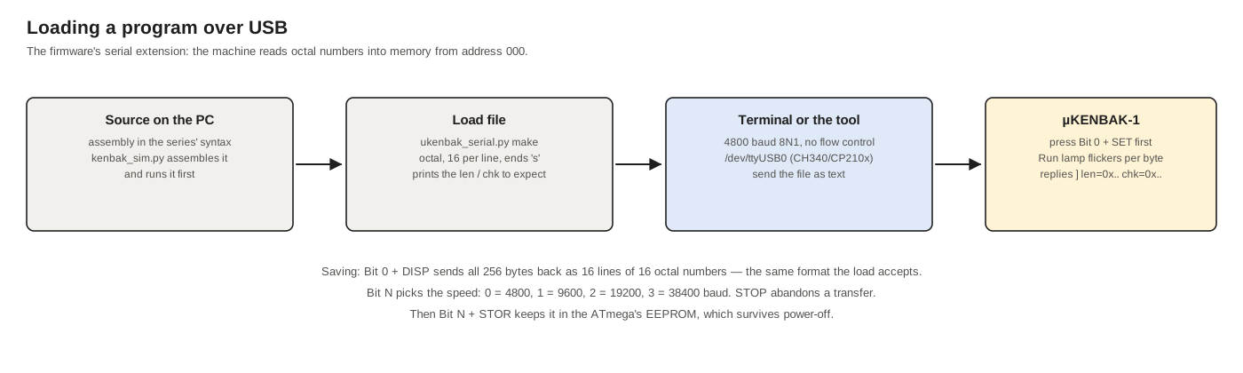
What the machine accepts, read from the firmware’s source (MCP.cpp):
- Octal numbers, separated by anything that is not a digit: commas, spaces, new lines. A leading 0 is harmless, so
0023and23are the same. - Hexadecimal numbers if prefixed
0x, with capital A–F. A lower-case letter ends the number; and a lower-caseeends the whole load. - The end: the 256th byte, a lower-case
eors, or the Stop key. - The report: when it finishes the machine sends a line such as
[0123] len=0x22 chk=0x67, the hex digits counting progress through memory, then the number of bytes stored and their sum modulo 256, both in hexadecimal. Comparing that line with the expected values is a complete check that the load arrived intact.
Three quirks of the reader are worth knowing. Hex needs the 0: x13 alone is read as octal 013. Octal digits 8 and 9 are treated as separators, so a stray decimal number is silently split. And a number left at the very end of the file without anything after it is stored but not counted in len, so a load file should always end with a separator and s.
A dump from data key 0 + Display is in exactly the format the reader accepts, sixteen lines of sixteen numbers like 0023,0001,0034,…, so a saved dump can be sent back unchanged.
A tool for it. The series’ tool ukenbak_serial.py (in 03-outputs/tools/) does the work at the computer end. It assembles a program written in the syntax of the series’ simulator, kenbak_sim.py, sets P to 004, writes the load file and prints the report the machine should give; it parses a dump back into a listing; and, with the Python pyserial package installed, it sends and receives directly. Its reader is a line-for-line copy of the firmware’s, and its self-test checks it against Wilson’s own published examples: his “Das Blinken Lights” load file in octal and in hex load the same 55 bytes, and his dump of the Sieve program parses and re-dumps character for character. The bouncing lamp of Volume 10, made into a load file by the tool:
$ python3 ukenbak_serial.py make v10_bounce --short
0000,0000,0000,0004,0023,0001,0034,0200,0364,0030,0311,0047,0006,0034,0200,0364,
0030,0111,0302,0000,0344,0015,0344,0006,0000,0224,0041,0213,0001,0243,0033,0354,
0030,0040,
s
# the machine should answer: ] len=0x22 chk=0x67
The first four numbers are A, B, X and P; P = 004 is where Start begins. The --short option stops at the end of the program (address 041) rather than writing all 256 bytes, so the rest of memory is left as it was; press Clear + Store first for a clean slate. Sent to a machine waiting on data key 0 + Set, it should answer len=0x22 chk=0x67, 34 bytes summing to 0x67; then Start runs it. In the simulator the lamps step 001, 002, 004, 010, 020, 040, 100, 200 and back.
Terminal settings on Linux. The module appears as /dev/ttyUSB0 (or the next free number). The user needs to be in the dialout group to open it. On Ubuntu 22.04 and later, the braille-display service brltty claims CH340 adapters by their USB identity and disconnects them a second after they appear; unless a braille display is in use, sudo apt remove brltty cures it (Ubuntu bug 1970408). Any terminal program will do for sending a file by hand: a µKENBAK-1 owner on the maker’s forum reports GTKTerm with no parity, eight data bits, one stop bit and no flow control (ukenbak-1 group). Note that the machine’s port runs at 38,400 baud at all other times, so a terminal left open at 4,800 will show nothing until a transfer starts.
13.8.3 Using the clock in a program
One short program shows the SysInfo call at work. It reads the clock’s seconds and shows them on the data lamps, as two BCD digits, over and over:
Loc  Contents  Label  Symbolic
003  004              P: start at 004
004  023       LOOP   LOAD A C=000     SysInfo index 000: seconds
005  000
006  360              SYSX             read the clock into B
007  134              STORE B OUTPUT   show it
010  200
011  344              JPD UNC LOOP
012  004
The listing is assembled by kenbak_sim.py (source 03-outputs/programs/v13_seconds.kas); the simulator runs it, but with 360 as a NOOP its lamps stay at zero, so the clock reading itself can only be seen on the kit. As a load file it is eleven bytes, len=0xB chk=0xCB. At 37 seconds past the minute the lamps show ○○ ●●○ ●●● (067, BCD 3 and 7), the pattern the simulator gives when B is preset to that reading.
13.8.4 Saving
Once a program is in, data key N + Store keeps it in EEPROM page N through power-off, and data key N + Read brings it back. Held at power-on, Read + key N makes the machine start that program every time it is switched on, which turns the kit into a clock or a display piece.
13.9 Rebuilding the Firmware
The kit never needs new firmware to work. It needs it to take Wilson’s later fixes, to cure the memory-lock fault on an early kit, or to change something. The maker’s method is simple: “there is no Arduino inside this project … the easiest way is to simply remove the ATMega328 chip from the µKENBAK-1 and replace the ATMega328 chip in an Arduino Uno, then upload like usual” (Adwater & Stir, “Kenbak Software Install”).
-
Get the source. Download Wilson’s repository from GitHub. If it arrives as
Kenbakuino-master, rename the folder toKenbakuino; the Arduino software requires the folder to match the sketch’s name. -
Make the one change the kit needs. The source assumes a DS1307 clock. For the kit’s DS3231, set the three constants near line 16 of
Clock.h, as the maker specifies:static const int RTC_I2C_ADDR = 0x68; static const int RTC_CONTROL_OFFSET = 0x0E; static const int RTC_USER_SRAM_OFFSET = 0x00;This step matters more than it looks. Left at the DS1307 values, the firmware would write its settings (auto-run, the user bytes, the key-toggle flag) into DS3231 registers 0x08 to 0x0F, which on that chip are its alarm and control registers. With the values above, the settings live in the top of the ATmega’s EEPROM.
-
Compile and upload for the board “Arduino Uno”. In the Arduino IDE that is the usual Upload; from the command line:
arduino-cli compile --fqbn arduino:avr:uno Kenbakuino arduino-cli upload --fqbn arduino:avr:uno -p /dev/ttyACM0 Kenbakuino -
Move the chips. Power both boards off. Lever the µKENBAK-1’s ATmega328P out of its socket evenly from both ends, put it in the Uno (notch to the Uno’s notch), upload, then return it the same way round. The Uno’s own chip goes back in the Uno.
Two other routes work without an Uno:
- An in-system programmer. A USBasp or an Arduino running the “Arduino as ISP” sketch writes the chip directly, through its SPI pins, either in a breadboard or in a 28-pin test clip. This also burns the Uno bootloader into a blank spare chip (Tools → Burn Bootloader in the IDE), which sets the Uno’s fuses (low 0xFF, high 0xDE, extended 0xFD: external 16 MHz crystal, 512-byte boot section).
- The DTR modification (untried). Wiring the module’s DTR pin to the ATmega’s RESET (pin 1) through a 0.1 µF capacitor would let the Arduino software reset the chip through USB, as on an Arduino Pro Mini, and upload in place. The chip must have the bootloader, and the pin is simply unconnected now, so this is a small, reversible change; it is not a documented modification and is listed here as an idea.
Before replacing the firmware, it is worth saving the old one. With a programmer, avrdude -c usbasp -p m328p -U flash:r:ukenbak-original.hex:i -U eeprom:r:ukenbak-eeprom.hex:i reads both out, so the kit’s own build, with whatever changes the maker made, can always be put back.
13.10 Faults and Fixes
Table 13 — Faults and Fixes
| Symptom | Likely cause | Fix |
|---|---|---|
| A key cap binds or does not click | The switch is off-centre in its panel hole | File or clip the cap’s “ears” (Volume 9); next time, solder the switches with the panel in place |
| A key works only sometimes | A cold joint on the switch or its pull-down; data and control keys are on different ‘165s | Reflow the switch’s four pins. Trace with the schematic: with the key held, its ‘165 input should read 5 V. Remember the scrambled order (data key 2 = pin G of the first ‘165) |
| Store does nothing; the lamp over Stop does not blink | Pre-August-2021 firmware reading a floating memory-lock input | A 10 kΩ resistor from ATmega pin 13 to pin 8, or new firmware |
| The clock resets to 12:00 after the power is switched off | Supply noise at the module as power goes, or a flat backup cell | Fit the 0.1 µF capacitor across the module; check the module’s cell |
| One data lamp dark | LED reversed or a bad joint; less often a ‘595 output | Test the LED with a meter’s diode range. Remember QA drives the left lamp (bit 7) |
| All data lamps wrong or frozen; control lamps fine | The ‘595 in the wrong socket or turned round | The ‘595 has its own socket between the ATmega and J1; notch to the right |
| Nothing lights at all | Power: the toggle’s wiring, the module’s pin order, or the ATmega out of its socket or turned round | The meter checks above. The crystal: a bad joint on Y1 stops the processor dead |
| Lights work, no serial port on the computer | A charge-only USB cable; the driver; brltty on Ubuntu | A data cable; the right driver for the module’s chip; sudo apt remove brltty |
A serial load reports the wrong len | A stray separator, decimal digits 8 or 9, lower-case hex, or a missing final separator | Check the file with ukenbak_serial.py check; send at 4,800 baud |
| Programs from the manuals run as a blur | The emulator is far faster than the original | Data key 3 or 4 + Stop |
| Auto-run or settings forgotten after re-flashing | Firmware built with the DS1307 constants | Rebuild with the Clock.h change above |
| Shift and P-register results differ from the books | Firmware older than May 2021 or September 2022 | Volume 9’s acceptance program; re-flash from the current source |
Two of these faults, the forgetful clock and the memory lock, appear in the maker’s addendum; the rest follow from the circuit. The maker’s forum lists several more threads from owners, among them a data lamp that would not light, traced by continuity testing, and an intermittent Stop key (ukenbak-1 group).
13.11 What I Will Add
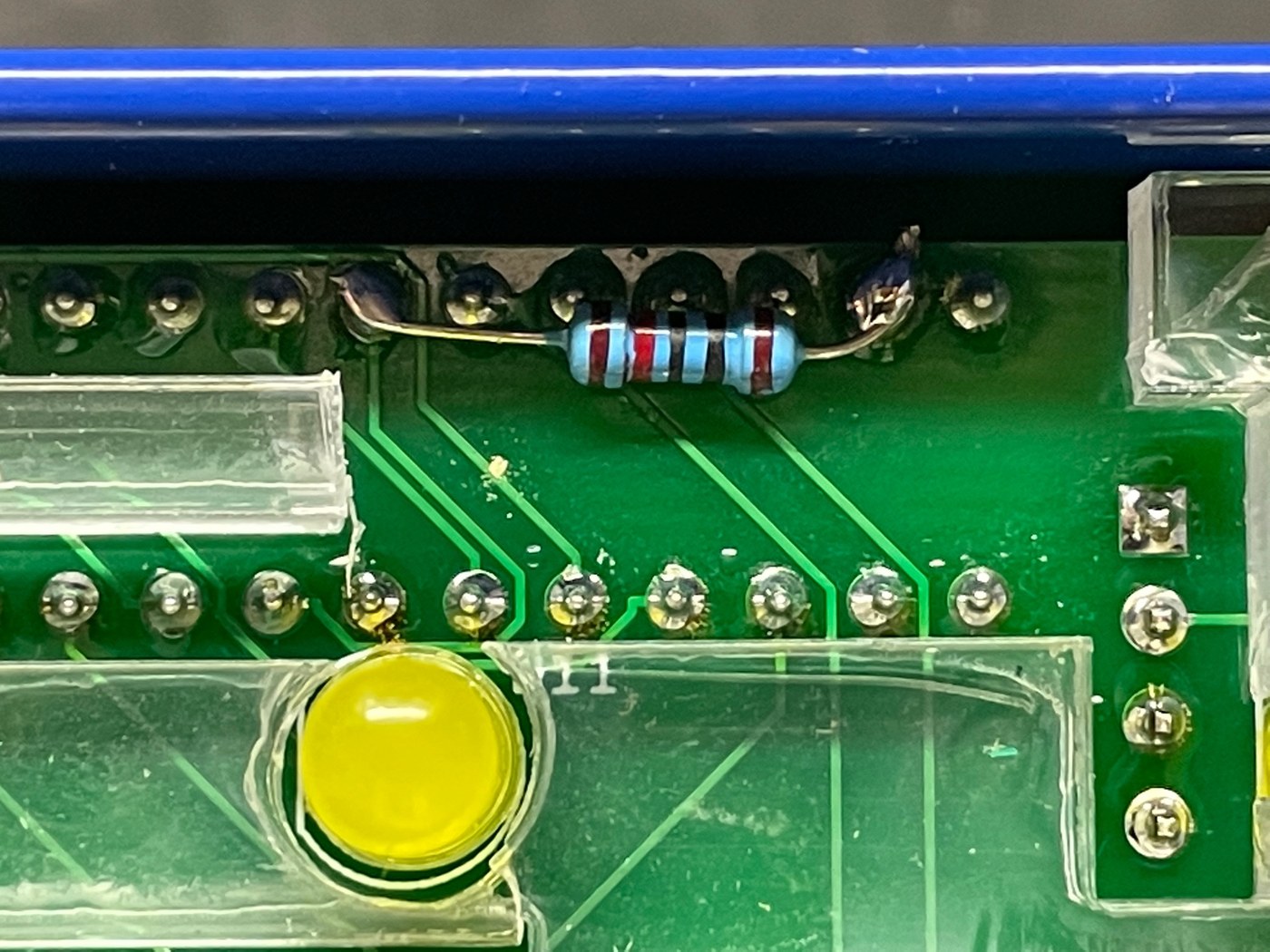
This volume is the reference; the record of my own µKENBAK-1 will fill in around it as the build goes.
13.12 Printable Bill of Materials
The whole parts list above is also a printable PDF for the bench: µKENBAK-1 BOM (PDF). Each part has a row with tick boxes for ordered, in hand and fitted, the quantity and where it goes, the part number to buy, alternates, where to buy it, its tag and space for notes. The last page is an order log.
Next — Volume 14: My nanoKENBAK-1. The same firmware on a board the size of a ruler: surface-mount parts, a rechargeable LIR2032 cell that must never be swapped for a CR2032, a clock chip with its own soldered backup cell, no serial port, and six unpopulated pads that are the only way to reach its processor.
Footnotes
-
Texas Instruments, SN74HC595 8-Bit Shift Registers With 3-State Output Registers, data sheet, https://www.ti.com/lit/ds/symlink/sn74hc595.pdf. ↩
-
Texas Instruments, SN74HC165 8-Bit Parallel-Load Shift Registers, data sheet, https://www.ti.com/lit/ds/symlink/sn74hc165.pdf. ↩
-
Bourns 4600X series SIP resistor networks: in the part number, 4610X = 10 pins, 4606X = 6 pins; -101 = bussed, -102 = isolated; the last three digits are the value (222 = 2.2 kΩ). Distributor listings, e.g. https://www.tanotis.com/products/bourns-4610x-102-222lf-fixed-network-resistor-2-2-kohm-100-v-5-elements-isolated-sip-300-mw. ↩
Comments (0)